Download
1 / 28
280 likes | 294 Vues
This paper explores the production, testing, and quality assurance process of the CMS Preshower Front-end Chips (PACE3). The paper discusses the features of PACE3, the production run, the test system, and the evaluation of the production run results.

E N D
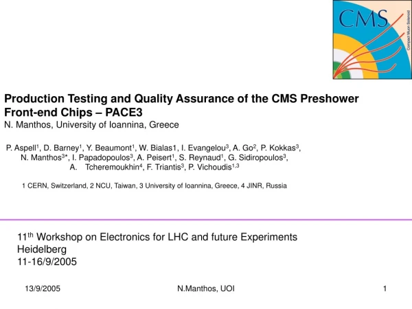
Production Testing and Quality Assurance of the CMS Preshower Front-end Chips – PACE3 N. Manthos, University of Ioannina, Greece • P. Aspell1, D. Barney1, Y. Beaumont1, W. Bialas1, I. Evangelou3, A. Go2, P. Kokkas3, • N. Manthos3*, I. Papadopoulos3, A. Peisert1, S. Reynaud1, G. Sidiropoulos3, • Tcheremoukhin4, F. Triantis3, P. Vichoudis1,3 • 1 CERN, Switzerland, 2 NCU, Taiwan, 3 University of Ioannina, Greece, 4 JINR, Russia 11th Workshop on Electronics for LHC and future Experiments Heidelberg 11-16/9/2005 N.Manthos, UOI
Outline • Introduction-CMS Preshower • PACE3 features • PACE3 production run • PACE3 test system • PACE3 production run evaluation • results • Summary and conclusions N.Manthos, UOI
CMS Preshower Geometry – physical location CMS N.Manthos, UOI
CMS Preshower active construction unit-Micromodule PACE3 N.Manthos, UOI
PACE principle specifications - Main Requirements from the CMS Preshower • PACE3C • 32-channel switchable-gain pre-amp/shaper with leakage-current compensation, • DC coupled to a single silicon sensor (50pF strip capacitance) with multiplexed • differential analog readout. • In addition includes: • an analogue pipeline memory (192 cells), storing data until reception of a level-1 • trigger (LV1). FIFO 48 deep (16 LV1s) • Internal injection circuit able to explore full dynamic range. • Programmable internal DACs for biases/currents etc. measured by connections • to external DCU. • PACE3C specs: • Dynamic range0.1 - 400 MIPs. • Linear response to energy (if possible) • Signal to noise ratio of 10 (for calibration using single MIPs). • S/N in high gain, HG (with sensor) of >6:1, HG dynamic range 0.1 – 50 MIPs • S/N in low gain, LG (with sensor) of ~2:1, LG dynamic range 1-400 MIPs • Good memory uniformity. • To avoid the need for many pedestals per channel • Operate at the LHC bunch crossing frequency of 40 MHz (peaking time ~25ns). • LV1 latency 3.2µs programmable. • 3 samples per LV1. • Possibility to store up to 16 triggers in memory. • Skip controller must be able to skip 15x3 consecutive cells etc. • Reasonable power consumption. • Reliable Programmability through I2C. N.Manthos, UOI
PACE3C Assembly of two ASICs Delta3 and PACEAM3 PACE3 unpackaged Technology: 0.25um CMOS Delta3 PACEAM3 Designers: P.Aspell W.Bialas D.Moraes M.Dupanloup Q.Morrissey Engineering run: Early 2005, tested at CERN, Yield ~80%,Yield relatively low due to chips from ALL reticles being packaged – including those at the boundaries of the wafers and some packages with only one chip! Package :196 fpBGA (15x15 mm) 1mm ball pitch Thickness = 1.7mm N.Manthos, UOI
PACE3 analog chain Internal Calibration Circuit (HP and LP) N.Manthos, UOI
HP, HG (< 10MIPs) LP, HG (< 50 MIPs) 3.1 LP, LG (< 400 MIPs) HP, LG (< 10 MIPs) Step response from the calibration circuit Output Voltage (V) HG LG ~ 400 MIPs equivalent 1.256 Calibration Circuit O/P Voltage Step 3.14 mV step = 1 MIP LP 1.5 50 400 0 Signal (MIPs) HP Overlap between the two gains to inter-calibrate. Match the response of a real MIP with electronic injection pulse Calibration of system with real single MIPs. Cal pulse… 1 to 50 MIPs 0 256 DAC CalV input value PACE3 Calibration Overlap between the two gains High Precision (HP) Range …. –31.4mV to 31.4mV, lsb = ~0.314mV (Range …. –10 to 10 MIPs, lsb = 1/10th MIP) Low Precision (LP) Range …. –31.4 mV to 1.256 V, lsb = 7.8 mV (Range …. –10 to 400 MIPs, lsb = 2.5 MIP) Will need to measure LP and HP response periodically to calibrate the calibration circuit. N.Manthos, UOI
The Reticle layout LSB MSB Laser blown 16 bit Chip ID register in Delta, PACEAM read by I2C Delta PACEAM K Unused Chip Type Wafer No. 6 bits Reticle X 4 bits Reticle Y 4 bits Delta PACEAM PACEAM Chip Type coding D P K 10 10 11 D P P 00 00 01 Note : Delta and PACEAM can be distinguished by reading control register 1 Production First production phase of packaging: 6 wafers ~ 1840 chips. 63! : rejected due to failure during packaging The Preshower needs 4300 PACE modules Production run is ~ 48 wafers ~ 150 reticles per wafer Giving : ~14K Delta chips ~21K PACEAM chips Package number (laser-printed on the package) 1xxxx, 0xxxx, engineering run wafers 2xxxx, 3xxxx : production run wafers N.Manthos, UOI
Evaluation of the production run chips • Tests overview • Initial tests • Power-on and check current (short circuits?), • basic i2c communication to chip • Digital functionality tests and default values to registers • Check all registers (write/read), flip-flops, • write default values to registers (Delta, PACEM) • Channel (groups of 8 channels) injection • tests (LGLP, V0cal=200), store the 2nd sample • (check full data path functionality in all channels). • Test and calibrate DACs – set optimum values for bias • voltages/currents • Linearity scan (for dynamic range, gain) • Timing scan • Optimum sampling point, shape, tp, tr, • Calibration procedure. Input from DACs scan - linearity • scan to estimate the gain. • Skip Controller, memory uniformity and noise in low gain, • noise in high gain. Standard test procedure Elapsed time ~4min/chip Total operator time ~6 min/chip including the chip insertion/take out from the ZIF socket, etc. N.Manthos, UOI
Test system • PACE3 Test board • Based on M16C μController • From Agilent E3631A • power supply, programmable • through RS232 by the PC • Pace3 supply lines • Programmable delay lines • FPGA Altera ACEX • ADC: AD41240 12-bit • DCU: DCU25F • To/from PC (RS232 or USB) PACE3 testing PACE3 ZIF socket PACE3 testing daughter board Hybrid testing daughter board N.Manthos, UOI Hybrid testing
Test system – user interface LabVIEW application N.Manthos, UOI
Initial tests Digital tests PACE power on current, run current , Power consumption Digital test and default registers 198 chips were rejected 13 overflow Passed chips Average Power on current = 38 mA Average Run current = 209 mA Average Power consumption = (209-38) mA x 2.5 V= 427.5 mW 14 chips were rejected Digital tests and updating registers N.Manthos, UOI
Channel Injection tests Injection of one event in all 32 channels (internal pulse) Normal response 14 chips were rejected 1st sample 2nd sample 3nd sample Rejected chip For hybrid tests: Ground bar in all channels. In case of no connection of a channel to bonding pad Injection Test failed One channel is not working N.Manthos, UOI
Setting PACE nominal biases DAC scan DAC spread for optimized values of V0Preamp, V0Shaper, Spare, VMemRef, VShift, VOutBuf PACE includes 13 8-bit DACs (Vref=2.5V) for bias voltages and currents. They are set to their nominal values and they are measured by the DCU. Example for V0Preamp 4 values set to DAC and measured by DCU, Fit. Slope: 3.96mV/DAC div Output of the voltage DACs through a divider to the DCU. Nominal V0Preamp=1.8V= 2 (due to the divider)*3.96*DAC value → DAC optimized value=227 Optimized values for: V0Preamp 232±2.6 V0Shaper 90±1.3 VMemRef 78±1 VShift 151±1.6 VOutBuf 158±2 Slope spread of Voltage DACs=0.04 mV/div Slope spread of Current DACs=0.12 mV/div N.Manthos, UOI
Linearity Scan Gain for LGLP,LGHP, HGLP,HGHP • Two gains and two precisions: • Pedestal run • 2 channels (time consuming proc) injected using full range of V0Cal DAC in steps of 2. • Pedestal subtracted 5 chips were rejected 1 underflow Passed chips Average Gain LGLP= 3.26 ± 0.03 mV/mip Average Gain LGHP= 3.16 ± 0.06 mV/mip Average Gain HGLP= 19.6 ± 0.3 mV/mip Average Gain HGHP= 19.7 ± 0.3 mV/mip N.Manthos, UOI
Timing Scan A0 0.9 A0 tr 0.1 A0 tp Shape of the pulse – rise time tr Using the delay line (IDT Y0207P) in the test system mother board. Find the optimum sampling point, channel to channel variation of the pulse shape Tune the time between ReSynch and Trigger signal. 25 steps of 1 ns N.Manthos, UOI
Timing Scan Rise Time (10 to 90%) for high and low gain, Peaking time Analysis to get the analogue parameters of the PACE chips has been performed using only the central time sample. Accepted Range (12-17 ns) No chips were rejected tp spread HG: 0.4 ns Average Rise time HG:15.2 ± 0.4 ns tp spread LG: 0.2 ns Average Rise time LG:13.2 ± 0.4 ns Average tp HG: 25.4 ± 0.4 ns Average tp LG: 23.0 ± 0.3 ns Uncertainty finding the start of the pulse N.Manthos, UOI
Calibration- DAC scan Dynamic range • Calibration: Conversion of the V0Cal to mips • for two gains two precisions. • One mip has been considered to be 3.5 fC (for a silicon sensor ~320 μm thick) • Input: data files from DAC scan • DCU ADC conversion factor: 0.465mV/DCU ADC count. • Take in to consideration the voltage divider between Delta and DCU: • factor= 1.375 for plateau, 1.875 for baseline. • mips=0.465(1.375*plateau-1.875*baseline)/3.14 • Input: data files from the linearity scans • Use of the AD41240 12-bit ADC (Input range 0-2.5V). • ADC conversion factor 0.435mV/ADC count. • mV=ADC counts *0.435 mV/ADC count • Fit a straight line to calculate the average gain • Store average gains and mips, mV N.Manthos, UOI
Calibration- DAC scan Dynamic range Slope of the fit curves : 1 N.Manthos, UOI
Calibration- DAC scan Dynamic range Max of the range for LGLP, HGLP where the deviation from the linearity <4% Deviation from linearity= 100*(Injected charge-measured charge)/injected charge LGLP HGLP N.Manthos, UOI
Skip controller Memory uniformity Noise test Skip mechanism test Send multiple triggers and verify that the skip mechanism works Analog memory 192 cells 0 … 191 trigger 1 trigger 2 5 chips were rejected trigger 3 trigger 4 trigger 5 Final trigger n in the test (5 in the drawing) is arranged so that the skipping mechanism must skip (n-1)x3 cells During the test 15 triggers are applied to block 15x3=45 consecutive cells, and a 16th one to skip the block of the 45 cells N.Manthos, UOI
Skip controller Memory uniformity Noise test DC spread and memory uniformity The rms of the average pedestal values of each channel in all memory cells. For each memory cell 27 events Chan-to-chan DC spread. 6 chips were rejected 11 overflow 6 overflow Low gain Passed chips Mean DC spread = 29 mV Average Memory Uniformity = 0.9 mV Pedestal rms of each channel through out the memory. 3 events/location Memory uniformity: average of the 32 rms. N.Manthos, UOI
Skip controller Memory uniformity Noise test Noise of a single cell in the memory for HG, LG No chips were rejected Passed chips Average noise HG 1.6 mV S/N=19.6/1.6=12.2 Average noise LG 1.1 mV S/N=3.26/1.1=3.0 N.Manthos, UOI
Test results – Yield # % yield(%) Chips(6 wafers) 1840 rejected due to failure during the packaging , 52 of them empty packages! 63 Received 1777 Tested 1776 Rejected393 22.1 77.9 Power on current out of spec ( 30 - 50 mA ): 189 10.6 Failed to read Delta/PACE-AM chip ids correctly 150 8.4 Digital tests failed 8 0.4 Update of PACE-AM registers failed 6 0.3 Run current out of spec (150 - 250 mA) 7 0.4 Current consumption out of spec (150 - 200 mA) 2 0.1 Injection test failed (all channels) 14 0.8 Gain in LGHP out of spec (2.8 - 3.4). 2 0.1 Gain in HGLP out of spec (18.5 – 22) 1 0.1 Gain in HGHP out of spec (18.5 - 22) 2 0.1 Memory uniformity out of spec (0 – 2 mV) 1 0.1 Channel-to channel DC levels out of spec(0-50mV) 5 0.3 Skip controller test failed 5 0.3 At least one channel has zero noise 1 0.1 The Yield could be increased to >95% If the 1st two reasons of failure can be resolved N.Manthos, UOI
Test results – Yield –map of the package-tested chips vs package number PACE production evaluation summary Passed production evaluation Failed production evaluation Failed during packaging. ~90% of them empty packages Not tested There are groups of rejected chips with adjacent package number. N.Manthos, UOI
Test results – Yield –packaged-tested chips vs their location in the wafer The Reticle layout Delta PACEAM K Delta PACEAM PACEAM Although the packaging company got the instruction to use chips (Delta and PACEAM) from the reticles with number 1 and 0, they have used chips near to the border of the wafer where we knew from the engineering run that they will have problems Dark: PACEAM not used for the production run (chip id=1) White: Delta and PACEAM used (packaged) for the production run N.Manthos, UOI
Summary and Conclusion • 1776 packaged PACE3 chips from the production run were extensively tested. • The test system developed for the production evaluation performs fine. • ~ 6 min are needed for the test of each chip. • Very small spread of gain, of pulse shape and noise observed between the chips. • Their dynamic ranges follow the specifications. • The production Yield is ~78%. • More study is needed to understand why the rejected chips are not passing those • tests which reducing the yield significantly. • The test data have been stored in the CRISTAL database. • Similar tests will be performed in the hybrid and micro-module level • using the same main hardware and software. • 38 more production run wafers (~38 x 300 PACE3 chips) exist. • Chips taken from more central area of the wafer from 20 wafers will be packaged at • the end of September. • They will be tested at Ioannina this autumn. N.Manthos, UOI