5 Packaging Intro
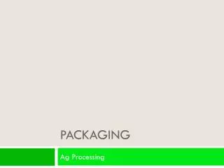
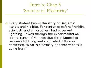
MEMS MOEMS Nano. Workshop. 5 Packaging Intro. Ken Gilleo PhD ET-Trends LLC. 44%. the. DEVICE. DEVICE. Reworkability. Enable repair. WIRING. WIRING. JOINING. JOINING. Automated Handling. Easy Testability. Easy Assembly. PROTECTION. Package. Chip to PCB Compatibility.

5 Packaging Intro
E N D
Presentation Transcript
MEMS MOEMS Nano Workshop 5 Packaging Intro • Ken Gilleo PhD • ET-Trends LLC 44%
the DEVICE DEVICE Reworkability Enable repair WIRING WIRING JOINING JOINING Automated Handling Easy Testability Easy Assembly PROTECTION Package Chip to PCB Compatibility - - - Objectives - - - Rerouting Performance Enhancement Thermal Management PROTECTION Standardization Low Stress Enable Mechanical Movement Selective Access to Environment MEMS
Packaging Change Drivers • Miniaturization • Area • Height • Weight • Performance • High lead count • High frequency; processors, RF • MEMS/MOEMS/Nano; a new technology cluster Reduction Boost New Requirements
~50 Years ~50 Years Devices Nano MOEMS Vacuum PERFORMANCE MEMS Solid State TIME
Basic Package Elements • Base; platform; chip carrier • 1st Level Interconnect (to chip) • Routing (can be optional) • 2nd Level Interconnect (to substrate/PCB) • Enclosure; encapsulant • Special features • Thermal management • Ports, windows, other
DIE Packages Element – cont. DIELECTRICS • Substrate/Platform/Enclosure • Rigid organic; BT, etc. • Flexible organic; polyimide • Ceramic/glass • Metal with insulation • Protection; enclosure, encapsulation, passivation • Chip Connections (1st level) • Wire bond • TAB • Integrated TAB • DCA; Flip Chip • PCB Assembly (2nd level) • Fusible: solder spheres/balls/bumps • Non-fusible: leads, pins, pads CONDUCTORS CONDUCTORS
Lead Frames • Metal – free standing or pre-inserted into dielectric • Framing structure removed later • Ceramic hermetic; used for MEMS • Plastic Near-hermetic; limited use for MEMS • Finishes for die attach/bonding • Ag • Pd • Au • Ni • Multiple
Chip Carriers Chip Carrier: a packaging system for electronic chips (IC’s) that provides protection and a practical means of connecting to circuitry. Fan Out: 2nd Level interconnect fans outward from 1st level Conductor and Dielectric Fan In: First - 1964 A flex-based package
Area Array Packages • Flip Chip • LGA (Land Grid Array); leadless chip carrier, QFN • PGA (Pin Grid Array) • BGA (Ball Grid Array) • Micro-BGA (CSP)
Advanced Packaging Types • Advanced BGAs • Flex-Based • MultiChip • CSP • Array Molded • Wafer-Level CSP and FC PRODUCTIVITY
Flip Chip • Perimeter for small I/O count • Area Array is much more effective MEMS MEMS potential Selective underfill
Ceramic Packages Used for MEMS Hermetic moderately expensive • Cofired • Cast • Molded • Open (non-hermetic); chip carrier
Organic Substrate • Rigid; mostly epoxies (resin-glass) • FR4 conventional • FR4 type non-halogenated • BT (Bismaleimide-triazine) • New non-epoxy halogen-free products • Flexible • Polyimide • LCP Limited use for MEMS Non-hermetic Lowest cost
Infineon MEMS mic + ASIC chip MultiChip Packages Traditional Stacked Single-Plane Cavity type used MEMS + ASIC, other
Packaging Steps • Bond die (chip) to base; die attach) • 1st Level connect chip; wire bonding • Enclosure; encapsulant
Wire Bonding (WB) • Most common connection • Gold ball bonding dominants (~ 93%) • Features • Programmable; handles die and package change • Very versatile • Universal method • Fast, automatic, equipment makers keeping pace • Fully mechanical process • Clean; no pollution, waste, hazardous materials • Well-suited for MEMS/MOEMS
Package Protection • Fabricated cavity enclosure; metal, plastic, ceramic • Transfer Molding Compounds (solids) • Glob Top; free flow encapsulant • Dam & Fill encapsulants • Cavity fill encapsulants • Underfill; 4 basic classes • Underfill + encapsulant • Injection molded cavity packages; near-hermetic Most can’t be used for MEMS
DIE CAP MEMS BGA encapsulants:for protection & handling Only suitable for capped MEMS
Session Summary • Packaging is very dynamic today • The package is all about metal & dielectrics • Challenges are greater than ever • Chip advances push performance • WLP is finally gathering momentum • MEMS is opening up a new packaging industry