Download

1 / 19
200 likes | 238 Vues
This document provides detailed insights into dimensioning the focal plane for HgCdTe detector material, including pixel size, assembly views, and grid layouts. It also delves into the management of stray light and critical considerations for the overall design.

E N D
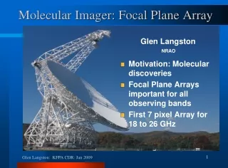
Dimensioning the focal plane(RSC centric version) C. Bebek 9 July 2003 Revised 14 July 2003
Rockwell HgCdTe detector material. 2048 x 2048 pixels. Pixel size 18 um. Note that photoactvice pixel count is 2040 x 2040. The four-pixel wide frame is read out for monitoring. This is the black band around the periphery. HgCdTe
A top view. The HgCdTe material is bump-bonded to a giant silicon circuit, blue in the drawing. The larger overhang at the bottom is where the output transistors, output amps, and some multiplexing exists. This is where the wire bond pads are also located. The overhangs on the other three sides are probably bussing for addressing the pixels but I do not know for sure. HgCdTe
This is the top view of the Lupinno moly package developed for Rockwell. The appendage at the bottom is the ceramic riser where wire-bonds attach to carry signals to the bottom of the package. Remeber the total height of 42.160 mm; this will drive the focal plane layout as we try to stack these into an array. HgCdTe
Total assembly, top view. Note that the silicon chip completely covers the moly mount face, to the accuracy I know the numbers. Fill-factor including rise 82.7%, 86.1% w/o. Wire-bonds span here. HgCdTe
CCD pixel area has been sized to match Rockwell HgCdTe pixel area. 3512 x 3512, 10.5 um pixels (matches 2048 x 2048, 18 um pixels) CCD
On the CCD silicon is the stuff to control the pixel reads. This is the dark green in the drawing. So, like the HgCdTe, there is a finite sized picture frame around the active region. Fill factor 88.8%. CCD
CCD on Luppino mount. How did it work out so well? Not an accident. Note, for the CCD the dimensions are the ideal diced size. In actuality the dicing is not precise. There is 50 um wiggle room total in the width and still not overhang the mount. Note, I have aligned the top edges of CCD and mount. With this, the photocenter for the CCD is 19.421 mm from the top and for the HgCdTe it is 19.190 mm. We can deal with this if we want absolute alignment of CCD and HgCdTe pixel areas. CCD pad edge pad edge
We diverge on a detail. The CCD could be rotated 900 relative to the mount from the previous slide. Effects Photocenter moves closer to the HgCdTe one by 280 um – can deal with it. The CCD overhangs the mount by 410 um – it will turn out that the mount width is constrained. The exposed mount height at the bottom imcreases from 1.061 mm to 1.618 mm. CCD
Gridding • To build a focal plane layout • Want the square photoactive region centers to lay on a square grid. • Guarantees stepping stars through the left and right arrays of the f.p. is in phase with stepping through the top and bottom arrays. • Guarantees that after 900 rotation, no stars that were being followed not get lost in cracks. • Remember biggest dimension of packaged devices is 42.160 mm. • Must leave some clearance for assembly. I use 1 mm in the following, but this was arbitrary and conversative. • Grids below are based on 43.160 mm.
TMA62 43.160 mm grid centered on f.p. Grid on F.P.
Why a grid, in one direction anyway? After stepping thru the bottom region, you want end up in the top region in the same relative pixel location. Populated F.P.
If you look close Photocenters are aligned. CCD packages are offset from HgCdTe ones to accomplish. 1 mm gap between ceramic riser and adjacent package. Big gaps between devices along the non-readout edges. 4.17 mm
Light up the cold plate to expose all places we need to worry about that can generate stray light.
Stray light management issues • As presently envisaged, all metal mounts are Au plated. • So there are many reflective canyons crisscrossing the f.p. • Advice sought • Is it important? • Trap light in the canyons? • Make mounts wider so there only slits between devices? • Treat non-photoactive surfaces? • Also issue of exposed wire-bonds on the top side – Luppino is aware of this.