UNIT-II Stick Diagrams
580 likes | 598 Vues
Stick Diagrams. UNIT-II Stick Diagrams. Stick Diagrams. Stick Diagrams. N+. N+. Stick Diagrams. V DD. V DD. X. X. X. X. Gnd. Gnd. Stick Diagrams. Stick Diagram. Stick Diagrams. V DD. V DD. X. X. X. X. Gnd. Gnd. Stick Diagrams. Stick Diagrams. Stick Diagrams.

UNIT-II Stick Diagrams
E N D
Presentation Transcript
Stick Diagrams UNIT-IIStick Diagrams
Stick Diagrams Stick Diagrams N+ N+
Stick Diagrams VDD VDD X X X X Gnd Gnd Stick Diagrams Stick Diagram
Stick Diagrams VDD VDD X X X X Gnd Gnd Stick Diagrams
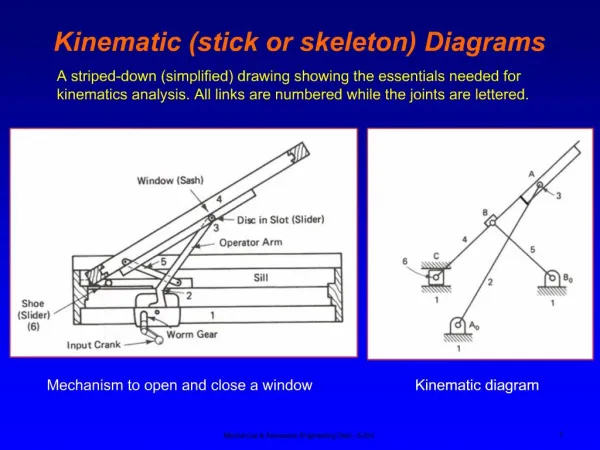
Stick Diagrams Stick Diagrams • VLSI design aims to translate circuit concepts onto silicon. • stick diagrams are a means of capturing topography and layer information using simple diagrams. • Stick diagrams convey layer information through colour codes (or monochrome encoding). • Acts as an interface between symbolic circuit and the actual layout.
Stick Diagrams Stick Diagrams • Does show all components/vias. • It shows relative placement of components. • Goes one step closer to the layout • Helps plan the layout and routing A stick diagram is a cartoon of a layout.
Stick Diagrams Stick Diagrams • Does not show • Exact placement of components • Transistor sizes • Wire lengths, wire widths, tub boundaries. • Any other low level details such as parasitics..
Stick Diagrams Can also draw in shades of gray/line style. Stick Diagrams – Notations Metal 1 poly ndiff pdiff Similarly for contacts, via, tub etc..
Stick Diagrams Stick Diagrams – Some rules Rule 1. When two or more ‘sticks’ of the same type cross or touch each other that represents electrical contact.
Stick Diagrams Stick Diagrams – Some rules Rule 2. When two or more ‘sticks’ of different type cross or touch each other there is no electrical contact. (If electrical contact is needed we have to show the connection explicitly).
Stick Diagrams Stick Diagrams – Some rules Rule 3. When a poly crosses diffusion it represents a transistor. Note: If a contact is shown then it is not a transistor.
Stick Diagrams Stick Diagrams – Some rules Rule 4. In CMOS a demarcation line is drawn to avoid touching of p-diff with n-diff. All pMOS must lie on one side of the line and all nMOS will have to be on the other side.
How to draw Stick Diagrams Stick Diagrams
Stick Diagrams Power A Out C B Ground
Introduction toCMOS VLSIDesignMOS devices: static and dynamic behavior
Outline • DC Response • Logic Levels and Noise Margins • Transient Response • Delay Estimation
DC Response • DC Response: Vout vs. Vin for a gate • Ex: Inverter • When Vin = 0 -> Vout = VDD • When Vin = VDD -> Vout = 0 • In between, Vout depends on transistor size and current • By KCL, must settle such that Idsn = |Idsp| • We could solve equations • But graphical solution gives more insight
Transistor Operation • Current depends on region of transistor behavior • For what Vin and Vout are nMOS and pMOS in • Cutoff? • Linear? • Saturation?
nMOS Operation Vgsn = Vin Vdsn = Vout
nMOS Operation Vgsn = Vin Vdsn = Vout
pMOS Operation MOS equations
pMOS Operation Vgsp = Vin - VDD Vdsp = Vout - VDD Vtp < 0 MOS equations
pMOS Operation Vgsp = Vin - VDD Vdsp = Vout - VDD Vtp < 0
I-V Characteristics • Make pMOS is wider than nMOS such that bn = bp
Load Line Analysis • For a given Vin: • Plot Idsn, Idsp vs. Vout • Vout must be where |currents| are equal in
Load Line Analysis • Vin = 0 MOS equations
Load Line Analysis • Vin = 0.2VDD
Load Line Analysis • Vin = 0.4VDD MOS equations
Load Line Analysis • Vin = 0.6VDD
Load Line Analysis • Vin = 0.8VDD
Load Line Analysis • Vin = VDD
DC Transfer Curve • Transcribe points onto Vin vs. Vout plot
Operating Regions • Revisit transistor operating regions
Beta Ratio • If bp / bn 1, switching point will move from VDD/2 • Called skewed gate • Other gates: collapse into equivalent inverter
Noise Margins • How much noise can a gate input see before it does not recognize the input?
Logic Levels • To maximize noise margins, select logic levels at
Logic Levels • To maximize noise margins, select logic levels at • unity gain point of DC transfer characteristic
Transient Response • DC analysis tells us Vout if Vin is constant • Transient analysis tells us Vout(t) if Vin(t) changes • Requires solving differential equations • Input is usually considered to be a step or ramp • From 0 to VDD or vice versa
Inverter Step Response • Ex: find step response of inverter driving load cap
Inverter Step Response • Ex: find step response of inverter driving load cap
Inverter Step Response • Ex: find step response of inverter driving load cap
Inverter Step Response • Ex: find step response of inverter driving load cap
Inverter Step Response • Ex: find step response of inverter driving load cap
Inverter Step Response • Ex: find step response of inverter driving load cap