Download
1 / 8
80 likes | 88 Vues
The report "3D IC and 2.5D IC Packaging Market by Packaging Technology (3D Wafer-Level Chip Scale Packaging, 3D TSV and 2.5D), Application (Logic, Memory, MEMS/Sensors, Imaging & Optoelectronics, LED), End User and Region - Global Forecast to 2028" The 3D IC and 2.5D IC packaging market is expected to reach USD 82.0 billion by 2028 from USD 49.3 billion in 2023, at a CAGR of 10.7% during the 2023u20132028 period.

E N D
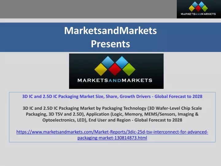
MarketsandMarkets Presents 3D IC and 2.5D IC Packaging Market Size, Share, Growth Drivers - Global Forecast to 2028 3D IC and 2.5D IC Packaging Market by Packaging Technology (3D Wafer-Level Chip Scale Packaging, 3D TSV and 2.5D), Application (Logic, Memory, MEMS/Sensors, Imaging & Optoelectronics, LED), End User and Region - Global Forecast to 2028 https://www.marketsandmarkets.com/Market-Reports/3dic-25d-tsv-interconnect-for-advanced-packaging-market-130814873.html
The 3D IC and 2.5D IC packaging market is estimated to be worth USD 49.3 billion in 2022 and is projected to reach USD 82.0 billion by 2028, at a CAGR of 10.7% during the forecast period. Growing adoption of high-end computing, servers, and data centers and miniaturization of IoT Devices are some of the major opportunities that lie ahead for the market. The semiconductor industry business is primarily driven by applications such as data centers/cloud, mobility, and the Internet of Things (IoT). The packaging technique must advance alongside the scaling of integrated circuit (IC) technology in order to fulfill the demands of next-generation information and communication technology (ICT) systems. Package design and development must simultaneously meet cost, performance, form factor, and reliability objectives. In terms of powering the design, the power density is higher for a given footprint than for traditional 2D chips. However, answering reliability issues will be crucial. Browse in-depth TOC on "3D IC and 2.5D IC Packaging Market" 124 – Tables 61 – Figures 224 – Pages
Consumer electronics to hold largest market share among end users in 3D IC and 2.5D IC packaging market Consumer electronics, by end user, is expected to hold the largest market share of the 3D IC and 2.5D IC packaging market. Increasing memory requirements in consumer products such as smartphones and tablets are driving the need for various advanced memories such as double-data-rate (DDR) dynamic random-access memory (DRAM), flash memory, and so on to be integrated. The advanced memory architectures are driving the demand for the 3D IC and 2.5D IC packaging market to offer high-performing, large-capacity, and compact products. Ask PDF Brochure: https://www.marketsandmarkets.com/pdfdownloadNew.asp?id=130814873 MEMS/Sensors to register highest CAGR in the 3D IC and 2.5D IC packaging market during forecast period The functional components of MEMS are micro sensors, micro actuators, and microelectronics. The advanced elements of MEMS are accelerometers, gyroscopes, digital compasses, inertial modules, pressure sensors, humidity sensors, microphones, and smart sensors, among others. The key requirement in all these elements and sensors is a miniaturized structure. Therefore, many sensors have started adopting 3D IC and 2.5D IC packages. 3D WLCSP to register highest CAGR in the 3D IC and 2.5D IC packaging market during forecast period 3D WLCSP is one of the most compact package types, with increased functionality and improved thermal performance in printed circuit boards compared to 3D TSV and 2.5D IC. 3D WLCSP has a simplified process design for manufacturing 3D ICs, which uses polymers that can sustain high temperatures, thus addressing the thermal issue, which is the major challenge for this market. 3D WLCSP has gained popularity in space-constrained consumer electronic applications and other portable consumer devices as well as industrial products as it offers cost-effective, small, lightweight, high-performance semiconductor solutions.
Asia Pacific held to register highest CAGR in the 3D IC and 2.5D IC packaging market during forecast period The Asia Pacific region is one of the key markets for 3D IC and 2.5D IC packaging owing to its broad scope in various consumer electronics applications, particularly in smartphones and tablets. This is mainly because of the high population density in the region, making it the largest potential market for 3D IC and 2.5D IC packaging among the four major regions. Request Free Sample Pages: https://www.marketsandmarkets.com/requestsampleNew.asp?id=130814873 Key Market Players The major players in the 3D IC and 2.5D IC packaging Companies include. The key players such as Samsung (South Korea), Taiwan Semiconductor Manufacturing Company, Ltd. (Taiwan), Intel Corporation (US), ASE Technology Holding Co., Ltd. (Taiwan), Amkor Technology (US), Broadcom (US), Texas Instruments Inc. (US), United Microelectronics Corporation (Taiwan), JCET Group Co., Ltd. (China) and Powertech Technology Inc. (Taiwan). These companies have used both organic and inorganic growth strategies such as product launches, acquisitions, and partnerships to strengthen their position in the market.
Driver: Growing demand for consumer electronics and gaming devices With the latest technological advancements, there are many new gadgets coming up in the market, such as e-book readers, gaming devices, tablet computers, 3D smart glass, augmented reality, and virtual reality products which demand high-performance electronic components. 3D IC packaging technology has helped bridge the processor memory performance gap by shortening the critical path and reducing the latency. It also allows scaling to continue efficiently by moving the focus from device-level scaling to circuit- and system-level scaling. Opportunity: Rising number of smart infrastructure and smart city projects 3D IC packaging can play a significant role in the development and implementation of smart city technology. Smart cities rely on a variety of electronic devices, sensors, and systems to collect and analyze data in real time, enabling better decision-making and more efficient resource management. By using 3D IC packaging, these devices and systems can be made smaller and more powerful and energy efficient. This helps reduce the overall cost and size of smart city infrastructure while improving performance and reliability. Challenge: Reliability challenges with 3D IC packaging The semiconductor industry business is primarily driven by applications such as data centers/cloud, mobility, and the Internet of Things (IoT). The packaging technique must advance alongside the scaling of integrated circuit (IC) technology in order to fulfill the demands of next-generation information and communication technology (ICT) systems. Package design and development must simultaneously meet cost, performance, form factor, and reliability objectives. In terms of powering the design, the power density is higher for a given footprint than for traditional 2D chips. However, answering reliability issues will be crucial.
About MarketsandMarkets MarketsandMarkets™ provides quantified B2B research on 30,000 high growth niche opportunities/threats which will impact 70% to 80% of worldwide companies’ revenues. Currently servicing 7500 customers worldwide including 80% of global Fortune 1000 companies as clients. Almost 75,000 top officers across eight industries worldwide approach MarketsandMarkets™ for their painpoints around revenues decisions. Our 850 fulltime analyst and SMEs at MarketsandMarkets™ are tracking global high growth markets following the "Growth Engagement Model – GEM". The GEM aims at proactive collaboration with the clients to identify new opportunities, identify most important customers, write "Attack, avoid and defend" strategies, identify sources of incremental revenues for both the company and its competitors. MarketsandMarkets™ now coming up with 1,500 MicroQuadrants (Positioning top players across leaders, emerging companies, innovators, strategic players) annually in high growth emerging segments. MarketsandMarkets™ is determined to benefit more than 10,000 companies this year for their revenue planning and help them take their innovations early to the market by providing them research ahead of the curve. MarketsandMarkets’s flagship competitive intelligence and market research platform, "Knowledgestore" connects over 200,000 markets and entire value chains for deeper understanding of the unmet insights along with market sizing and forecasts of markets.
Contact Us Contact: Mr. Aashish Mehra MarketsandMarkets™ INC. 630 Dundee Road Suite 430 Northbrook, IL 60062 USA : 1-888-600-6441 For More Info: https://www.marketsandmarkets.com/PressReleases/3dic-25d-packaging.asp