Download
1 / 5
60 likes | 196 Vues
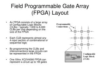
This work, achieved in collaboration with Aaron Egier, Ketan Padalia, Ryan Fung, and Mark Bourgeault, and supervised by Jonathan Rose, presents a groundbreaking automatic layout design flow for Field Programmable Gate Arrays (FPGAs). Traditional FPGA design is time-intensive, often requiring over 50 person-years for completion. Our automated method reduces this time significantly to just 34 person-weeks, showcasing a major leap in efficiency. We detail our GILES CAD flow, highlight chip specifications (0.18 µm process, 358,374 transistors), and discuss future directions for further automation and transistor sizing.

E N D
Automated FPGA Layout Ian Kuon Work done in conjunction with Aaron Egier, Ketan Padalia, Ryan Fung, Mark Bourgeault Supervised by Jonathan Rose
Challenge • Making ASICs is hard • That’s why we use FPGAs! • Making FPGAs is even harder • >50 person-years for a new FPGA
The GILES CAD Flow # Logic block parameters subblocks_per_clb 1 # 1 BLE per logic cluster subblock_lut_size 4 # 4-input LUTs # Logic block inputs and outputs inpin class: 0 bottom inpin class: 0 left inpin class: 0 top inpin class: 0 right outpin class: 1 bottom # Logic block output inpin class: 2 global left # Clock input # Connection block flexibilities Fc_type fractional # Specified as fractional number of tracks Fc_input 0.5625 # Flexibility of input connection block Fc_output 1 # Flexibility of output connection block Fc_pad 1 # Flexibility of I/O pads # Switch types switch 0 buffered: no ... switch 1 buffered: yes ... # Length 4 routing tracks, half buffered segment frequency: 0.5 length: 4 wire_switch: 0 ... segment frequency: 0.5 length: 4 wire_switch: 1 ...
Summary • Chip made in 0.18 um process • 358,374 transistors • Significant time savings • 34 person-weeks vs. > 50 person-years
Future Directions • Further automate FPGA design • Transistor sizing