Download
1 / 27
340 likes | 619 Vues
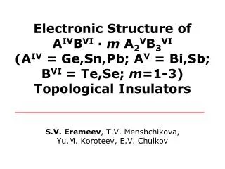
Electronic Structure of A IV B VI · m A 2 V B 3 VI (A IV = Ge,Sn,Pb; A V = Bi,Sb; B VI = Te,Se; m =1-3) Topological Insulators. S . V . Eremeev , T . V . Menshchikova , Yu . M . Koroteev , E . V . Chulkov. Outline. 1- Introduction to topological insulators 2- Motivation

E N D
Electronic Structure ofAIVBVI · m A2VB3VI(AIV = Ge,Sn,Pb; AV = Bi,Sb; BVI = Te,Se; m=1-3) Topological Insulators S.V. Eremeev, T.V. Menshchikova, Yu.M. Koroteev, E.V. Chulkov
Outline 1- Introduction to topological insulators 2- Motivation 3- New family of ternary topological insulators 4- Summary and conclusions
Introduction Topological insulators are one of the materials of the moment. In these unusual substances, the bulk behaves like an insulator, whereas the surface acts like a conductor. In addition to a host of practical applications, topological insulators are particularly important because they enable scientists to investigate a plethora of exotic states. Electrons in topological insulators are able to flow only at the edges of the material, not in the bulk. NPG Asia Materials featured highlight doi:10.1038/asiamat.2010.188
Introduction • Classification of materials according to band theory, Metalsl Semi-metalsl Insulatorsl E(k) EF k • But the quantum world can present more complex materials like, • * Superconductors • * Magnetic Materials • * Topological Insulators
Introduction Exotic properties • - Insulating bulk but metallic surface due to strong spin-orbit interaction. • Unique surface state that make surface conducting, with linear dispersion forming a Dirac Cone with a crossing point at the Fermi level. • Helical spin structure with the • spin of the electron • perpendicular to its • momentum. • Electrons in this surface state are protected against scattering. • Very promising for spintronics or quantum computing applications.
Discovery of TI and motivation 1st Generation : HgTe Q. Wells (2D), BixSb1-x (3D) Bernevig et al. Science 314(2006), Koenig et al. Science 318(2007), Fu and Kane PRB 76(2007), Hsieh et al. Nature 452(2008) 2nd Generation: Bi2Se3, Bi2Te3, Sb2Te3 3D crystals Zhang et al. Nat. Phys. 5(2009), Xiao et al. Nat. Phys. 5(2009), Chen et al. Science 325(2009) 3rd Generation: Ternary Bi2Se3- and Bi2Te3-based compounds (Bi2Te2Se, PbBi2Te4…), Heusler Compounds (Li2AgSb, NdPtBi…), Tl-based Bi chalcogenides (TlBiSe2, TlBiTe2), antiperovskite nitride (M)3BiN (M = Ca, Sr, Ba),honeycomb-lattice chalcogenides LiAgSe and NaAgSe, Pyrochlores…
Discovery of TI and motivation 2nd Generation: Bi2Se3, Bi2Te3, Sb2Te3 3D crystals Zhang et al. Nat. Phys. 5(2009), Chen et al. Science 325(2009)
Discovery of TI and motivation Why look for more Topological Insulators??? • Bi2Se3 Dirac Point is close to the Bulk Valence Band • maximum scattering channels (S. Kim et al, PRL 107, 056803 (2011)) • hexagonal warping of the Dirac cone: • more accurate • quasi-particle GW • approach reveals • several cases where • DFT identifications • of TI phases are • false Intrapair scatterings in (a) and (b) are forbidden by timereversalsymmetry. But interpair scatterings in (b), for example,those between k2 and k3, are allowed. (L.Fu, PRL 103, 266801 (2009)) J. Vidal et al, PRB 84, 041109(R) (2011)
AIVBVI · m A2VB3VI(AIV = Ge,Sn,Pb; AV = Bi,Sb; BVI = Te,Se; m=1-3) ternary compounds In this work the electronic structure of AIVBVI · m A2VB3VI(AIV = Ge,Sn,Pb; AV = Bi,Sb; BVI = Te,Se; m=1-3) series of ternary compounds are analyzed. The electronic structure was calculated in the density functional theory formalism as implemented in VASP. Like A2VB3VI these compounds have layered structure with ionic-covalent bonding within layers and van der Waals gaps between them, but unlike the parent compounds with simple quintuple layers structure, the structure of the ternary compounds contains alternating in various sequences quintuple and septuple layers. Peculiarities of bulk spectrum of these more complex materials give rise to more complicated surface band structure that depends on surface termination, which can be quintuple- or septuple-layer terminated. We predict the existence of exotic buried topological surface states which are characterized by a deep subsurface localization and Dirac states with the Dirac point in the valence band gap. Beside the Dirac cone states, which are peculiar to topological insulators, unoccupied Rashba-type spin-split state and occupied surface states can reside in these systems. We analyze dispersion and spatial charge density localization of the surface states. We also performed a layer-by-layer analysis of the spin distribution in the surface states.
Classification of topological phases Three-dimensional materials with inversion symmetry are classified with four Z2 topological invariants 0; (1, 2, 3), which can be determined by the parity m(i)=±1 of occupied bands at eight time-reversal invariant momenta (TRIM) i =(n1,n 2,n3) = (n1 b2 + n2 b2 + n3 b3)/2, where b1, b2, b3 are primitive reciprocal lattice vectors, and nj = 0 or 1 [1, 2]. The Z2 invariants are determined by the equations and where For rhombohedral lattice the TRIMs are ,Z, and three equivalent L and F points. 0=1 characterize a strong topological insulators. [1] L. Fu, C.L. Kane, and E.J. Mele, Phys. Rev. Lett. 98, 106803 (2007). [2] L. Fu, and C.L. Kane, Phys. Rev. B 76, 045302 (2007).
The topological number 0 for n AIVBVI · m A2VB3VI (n=1; m=1–3) compounds based on Bi2Te3, Sb2Te3 and Bi2Se3 parent phases Planar Perp.
parent compound Bi2Te3 SOC-induced band inversion marked by green ellipse
parent compound Bi2Te3 layer-resolved spin structure surface band structure of Bi2Te3 and spatial charge density distribution of the Dirac state NATURE 460, 1101 (2009).
Bulk band structure of PBT compounds SOC-induced band-gap inversion in PbBi2Te4 More complicated band structure in PbBi4Te7
Surface band structure of PbBi2Te4 Layer-resolved spin structure of the Dirac state in the topmost 7L block of PbBi2Te4, given by spin projections Sx, Sy, and Sz at 30 and 90 meV above DP. counter-clockwise spin rotation in the topmost Te atom
Surface band structure of n AIVBVI · m A2VB3VI (n=1; m=1)
Surface band structure of 7L-terminated PbBi4Te7(0001) counter-clockwise spin rotation in the topmost Te atom The character of p states changes from dominating py and pz in all subsurface layers to px in the topmost Te layer which can change the spin-orbit interaction and reverse the spin orientation.
Surface band structure of 5L-terminated PbBi4Te7(0001) Charge density distribution of the occupied and unoccupied surface states integrated over xy planes
Surface band structure of 5L-terminated PbBi4Te7(0001) Layer-resolved spin structure of the Dirac state at 5L-term PbBi4Te7(0001) at 100 meV. Spin projections for occupied SS
Surface band structure of n AIVBVI · m A2VB3VI (n=1; m=2)
Surface band structure of 7L-terminated and 5L-terminated PbBi6Te10(0001)
Summary and conclusions — We have shown that, in the homologous series of ternary compounds based on Bi2Te3, Bi2Se3 and Sb2Te3, most of the compounds AIVBVI · m A2VB3VI(AIV = Ge,Sn,Pb; AV = Bi,Sb; BVI = Te,Se; m=1-3) are 3D topological insulators. — Part of these systems (m = 2,3) represent naturally grown superlattices composed of 5L and 7L blocks, which demonstrate much richer physics than the parent TIs. — More complex surface electronic and spin structures, originating from peculiarities of the bulk spectrum of these materials, provides an efficient way to manipulate both the spin structure and the spatial localization of the conducting state. This subsequently may allow for a variation of the depth of the spin transport channel below the surface. References: С.В. Еремеев и др., Письма в ЖЭТФ, т. 92, с. 183 (2010), S.V. Eremeev et al., Nature Comm. 3:635, DOI: 10.1038/ncomms1638 (2012), Kuroda et al. PRL (under reviewing)
Prospective devices Structure of proposed memory cell, based on a TI block with a magnetically doped surface. A bit is stored by the perpendicular magnetization of the surface. Gate-tuned normal and superconducting transportat the surface of a topological insulator T. Fujita et al., Applied Physics Express 4 (2011) 094201 B. Sacepe et al., Nat. Comm (2011)