Download
1 / 23
230 likes | 416 Vues
NANOTECHNOLOGY: THE NEXT BIG REVOLUTION Dr. Albert Lozano Program Head Nanotechnology Program Commonwealth College The Pennsylvania State University. WHAT IS NANOTECHNOLOGY? Building very small structures namometer scale (nm) Human hair: 50,000 nm across

E N D
NANOTECHNOLOGY: THE NEXT BIG REVOLUTION Dr. Albert Lozano Program Head Nanotechnology Program Commonwealth College The Pennsylvania State University
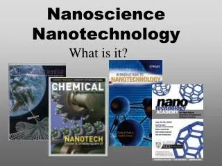
WHAT IS NANOTECHNOLOGY? Building very small structures namometer scale (nm) Human hair: 50,000 nm across Bacteria: About 200 nm across 10 Hydrogen atoms lined up: 10 nm Unaid human vision: 10,000 nm Nanotechnology: Build structures 1 to 100 nm
WHY NANOTECHNOLOGY? • Use atomic properties of materials • Less is more in medicine • Increase power of computer chips • Sensors responding to lower concentrations • Stain-resistant clothing • Bathroom coating: self-cleaning !!! • New applications being implemented • almost daily (www.smalltimes.com) • Integrate biology, chemistry, eng…
NANOTECHNOLOGY in the US Jan 2000: President Clinton developed the National Nanotechnology Initiative: $227 M increase funding Dec. 3, 2003: President Bush signed 21st Century Nanotechnology Research and Development Act $ 3.7 Billion over 4 years NNI: One of the few Clinton-era programs strongly backed by Bush Administration Bipartisan support: Senator Joseph Lieberman and former Speaker-of-the-House Newt Gingrich
BECOMING INVOLVED IN NANOTECHNOLOGY Ph.D. Research & MS. Development BS. Current applications AAS. Support Educational Opportunities at all levels within Penn State
CAREERS IN NANOTECHNOLOGY Education and academia Agriculture Food and beverage industries Environmental monitoring Communications and media Aerospace Electronics Information technology Many new industries the are emerging as a result of advances in nanotech
ApplicationsBiotechnology Microarrays – gene expression studies DNA sequencing through micropores (sequence the entire human genome in 2 hr instead of 3 years). Medicine Personalized medicine Microfluidics (a miniaturized laboratory) Synthesis of extremely small probes that can examine individual strands of DNA for disease detection. Man-made capillary systems to bring nutrients to artificial organs.
ApplicationsEngineering Manufacturing extrenely strong fibers atom by atom Very small valves Aerospace engineering Homeland Security Nanostructures as incredibly sensitive chemical and biological substance detectors (nanosensors) Information technology
ApplicationsEngineering Current advances in semiconductor electronics come through nanoelectronics state-of-the-art conventional transistor is now only about 100 nm in length Everyday life Flat, picture-like televisions and computer screens Pollution detectors Food bacteria detection Textiles Automotive / Transportation
PENN STATE - COMMONWEALTH COLLEGE • APPROACH TO NANOTECHNOLOGY • Associate of Applied Science Degree • In Nanofabrication Manufacturing Technology • Engineering Technology Option • Science Option • Currently developing a Baccalaureate Degree • Seamless transition for AAS graduates • 3 Semesters Home Campus • (WB, FY, HZ, MK, YK) • 1 Semester Nanofabrication Facility (UP)
PENN STATE – COMMONWEALTH COLLEGE • 3 semesters Home Campus • Develop skills to work in clean room facilities • Electronics, Science, Math skills • Plus PSU General Education requirements • 1 semester at University Park Campus • at Nanofabrication Facility • $32 million dollar, state-of-the-art laboratory • Hands-on experience all semester • Work with industry equipment Productive • University Park residential living
PENN STATE – COMMONWEALTH COLLEGE 2NMT / ET Option
PENN STATE – COMMONWEALTH COLLEGE 2NMT / Science Option
Introduction to Nanotechnology Quality Control and QualityAssurance 1 credit Taught at local campus Intro to modern statistical quality control methods used by industry. Recommended by Technical Advisory Committee Topics include: Q.C. concepts, principles, procedures, statistical tools, Statistical control of nanofabrication manufacturing and production processes and systems.
Introduction to Nanofabrication Manufacturing Technology Three credits Taught at local campus Gives an overview of atomic physics and the use of atoms to build devices and machines Topics include: Atoms Semiconductors Transistors Integrated circuits Basic Nanofabrication Processes The Nanotech industry
NANOFABRICATION FACILITY $32 million, state-of-the-art facility Professional engineering staff Class Ten Cleanrooms Broad spectrum of equipment Shared by educational institutions across the Commonwealth Three capstone semesters each year Facility available to industry.
NANOFABRICATION FACILITY Electron beam lithography and optical lithography Plasma etching tools Plasma deposition tools Physical vapor deposition equipment Chemical vapor deposition equipment Ion implanter
Capstone Courses Materials, Safety, and Equipment Overview for Nanofabrication Basic Nanofabrication Processes Thin Films in Nanofabrication Advanced Lithography and Patterning Techniques Materials Modification in Nanofabrication Characterization, Packaging, and Testing of Nanofabricated Structures
PENN STATE COMMONWEALTH COLLEGE:FUTURE DIRECTIONS Development of a BS in Science with a Nanoscience option (Fall 2005) Nanotechnology EXPO High school counselors, science teachers and students Technical advisory committee at each campus Nanoscience 001-natural science elective for all students Nanotechnology module for first year Engineering Design and Graphics (EDG 100) course
JOB MARKET IN NANOTECHNOLOGY • The next Industrial Revolution • Media reports to sense National Interest • AAS Graduates ranging $35k - $46k • Only area other than homeland security that • experienced increased growth in federal spending • Private sector spent $2 billion in 2002 • Opportunities for dual degrees: • 2EET and 2NMT in 5 semesters
PROFESSIONAL OPPORTUNITIES FOR 2NMT GRADUATES (where are the jobs?) Pharmaceuticals Biomedical Micro-electromechanical devices (MEMs) Opto-electronics (fiber-optic communications) Sensors Power electronics Microelectronics (chips) … and many more to come!
PROFESSIONAL OPPORTUNITIES FOR 2NMT GRADUATES (where are the jobs?) Pennsylvania nanofabrication workforce development program Workforce development program is the Pennsylvania Nanofabrication Manufacturing Technology (NMT) Partnership Two-year degree graduates of the “capstone experience” are receiving salary offers in the $30,000 - $52,000 range Baccalaureate graduates have starting salaries averaging $62,000