Download

1 / 1
20 likes | 272 Vues
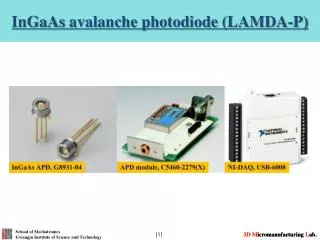
M. Ordinary photodiode. Linear-mode APD. Geiger-mode APD. 100. 10. 1. 0. Breakdown. Response to a photon. ∞. I(t). M. 1. Characterization of a Geiger-mode Avalanche Photodiode. Chris Maloney a Advisors: Dr. Don Figer b , Dr. Rob Pearson a , Dr. Sean Rommel a. Afterpulse.

E N D
M Ordinary photodiode Linear-mode APD Geiger-mode APD 100 10 1 0 Breakdown Response to a photon ∞ I(t) M 1 Characterization of a Geiger-mode Avalanche Photodiode Chris MaloneyaAdvisors: Dr. Don Figerb, Dr. Rob Pearsona, Dr. Sean Rommela Afterpulse May 10, 2011 Laser-induced firing APD current aRochester Institute of Technology, Department of Electrical and Microelectronic Engineering; bRochester Imaging Detector Laboratory APDbias Varm Timing gate Results Array Tested A 32x32 array of 100 µm silicon Geiger-mode APDs was designed and fabricated at MIT’s Lincoln Laboratories. The Rochester Imaging Detector Lab (RIDL) was given the responsibility to test and characterize the array. Objective The objective of this project was to extract key parameters that will allow for effective and efficient operation of a Geiger-mode avalanche photodiode (APD) array in a light detection and ranging (LIDAR) imaging system. tdead Fig. 6. Measured forward diode characteristic. Motivation LIDAR imaging systems can be used for a variety of applications. The most common is altimetry. Measuring the altitude of an object can be useful for observing celestial bodies, polar ice caps or ocean levels. In addition, this imaging system can be implemented in autonomous landing systems. • Ideality factor of n = 1.0 • No recombination/generation region • Series resistance ~2 kΩ Fig. 7. Dark count rate vs. bias. • Breakdown voltage ~32 V • Geiger-mode operation ≥ 32 V Fig. 3. Actual array of Geiger-mode APDs. • Camera Design • Requirements • Light tight • Allow for thermoelectric cooler • Mountable lens for imaging • Connector interface for existing hardware • Probeable hardware without disassembly Fig. 9. Measured afterpulsing. Fig. 8. Theoretical afterpulsing. • No afterpulsing is seen • Short trap lifetimes show a steep peak • Long life times exhibit a shallow peak • Deep level traps have long lifetimes and have a minimal effect on afterpulsing Fig. 4. CAD camera design (left); actual fabricated camera (right). Fig. 1. Enhanced LIDAR image of Mars (Image Credit: MOLA Science Team and G. Shirah, NASA GSFC Scientific Visualization Studio). Geiger-mode Operation APDs can be operated in linear-mode or Geiger-mode. Geiger-mode operation means the diode is biased at or just above the breakdown voltage of the device. This ensures single-photon sensitivity of the device. Fig. 10. Complete LIDAR system ready for imaging. Conclusions It was expected to see the results that were measured in the afterpulsing experiment. From the forward diode characteristic, no recombination/generation region was seen, implying that there are a minimal amount of traps in the device. Either there are no traps in the device or the lifetime makes the peak too shallow to see or so steep that it occurs before the shortest dead time. RIDL now has the means to test for afterpulsing in devices that MIT will be sending them in the coming months. Afterpulsing Afterpulsing occurs when an event is seen during a timing gate, and the dead time before the next timing gate is not long enough to account for the discharge of trapped charge. A false event will be seen. Acknowledgements I would like to thank Dr. Figer, John Frye, Dr. Rommel, Dr. Pearson and Dr. Hirschman for their help during this project. This work has been supported by NASA grant NNX08AO03G. Fig. 5. Waveform demonstrating afterpulse test. λ(tdead) – Dark count rate with respect to dead time Rdark – Dark count rate measured without afterpulsing Pa – Avalanche probability Nft – Number of filled traps τtrap– Trap lifetime tdead – Dead time Fig. 2. Comparison of photodiode operation (Image Credit: Dr. Don Figer). Eq. 1. Dark count rate with respect to dead time.