Test Conditions
Data Retention Bake. Test Purpose Data Retention Bake tests are performed to ensure the performance of data stored in memory devices, such as EPROMs. These type of tests measures the ability of the floating gate of the product to retain data. Test Principle

Test Conditions
E N D
Presentation Transcript
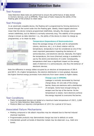
Data Retention Bake • Test Purpose • Data Retention Bake tests are performed to ensure the performance of data stored in memory devices, such as EPROMs. These type of tests measures the ability of the floating gate of the product to retain data. • Test Principle • In an electrically erasable device, the floating cell is programmed by forcing electrons to tunnel through the tunnel oxide into the floating gate. Ideally, these trapped electrons mean that the device remains programmed indefinitely. Actually, the charge cannot remain indefinitely, but its lifetime is normally extremely long. The stability of the program charge is known as data retention—i.e., the ability of the device to retain its charge as programmed, or to retain its data. • Temperature Dependence of SemiconductorsSince the average energy of a solid, and its components (atoms, electrons, etc.), is in direct relation with its temperature, temperature must be considered as one of the most important parameters impacting the behavior of semiconductors, and electronic devices. Basically, the higher the temperature, the more (thermal) energy is available for use by the atoms and electrons of a solid. Consequently, temperature shall have a significant impact on the energy state of electrons in a semiconductor, and thus the behavior of electronic devices. • Note the difference in energy states occupied by an electron at temperatures of 300 K and 604 K. At a higher temperature, the electron distribution is more gradual, because the higher thermal energy promotes more electrons from lower states to higher states. Charge Loss in EPROMs Leakage is normally dominated by thermal charge decay. On one side of the energy barrier, there are electrons with a distribution of energies. Some have enough energy to escape over the top of the barrier. As the temperature is raised, more electrons achieve the energy required to overcome the barrier. • Test Conditions • Plastic encapsulated devices are tested at a maximum bake temperature of 150C, 2,000 hours for Data Retention Bake testing. • Moisture Bake-out requires a temperature of 125C for a period of 24 hours. • Associated Failure Mechanisms • Molding compound or die attach impurities may be released due to thermal induced chemical reactions. • Programmable products may demonstrate charge loss due to defects on oxide. • Interdentally growth at bonds of dissimilar metals may be observed—e.g., Gold wire bonds.
delamination b Delamination Temperature Cycle • Test Purpose • Temperature Cycle (TC) test, also called Temperature Cycling, determines the ability of integrated circuits components and solder interconnects (of electronic assemblies) to withstand the mechanical stresses induced by the alternating high and low temperature extremes. • Test Principle • TC test is an accelerated test by which IC packages are exposed to a number of cycles of extreme air temperatures that may be as low as 65°C and as high as 150°C. Thermal cycling is likely to initiate mechanical fatigue degradation mechanism in all circuit materials, but the processes are greatly accelerated where mechanical or chemical defects have created stress concentrators—e.g., microcracks, hard precipitates, and abnormally thin features. • Test Conditions • -55°C~125°C • -40°C~150°C • 1-3 cycles per hour Cracked Passivation Associated Failure Mechanisms • Cracked packages and die • Cracked passivation and thin film • Broken or sheared bond wires and bonds • Bond pad cratering • Die attach separation or failure • Interlayer dielectric voids or cracks • Stress-induced metallization voids • Displaced metallization • BGA substrate damage to trace and via • BGA–beam lead damage • Loss of hermeticity on hermetic package Passivation Damage Sheared Ball Bonds Ball Neck Broken Die Top Delamination
High Temperature Operating Life • Test Purpose • High Temperature Operating Life (HTOL) Tests, also known as Steady-state life tests, are performed for the purpose of demonstrating the quality or reliability of devices over an extended period—i.e., to estimate the useful life of a product under normal operating conditions. • Test Principle • HTOL tests are accelerated tests by which IC packages are subjected to electrical tests that simulate normal operating conditions, performed at elevated temperatures to provide thermal acceleration. The tests are specifically designed to evaluate the different portions—i.e., early life, inherent life, and extended life—of the useful life of a product where parts with manufacturing defects would fail. • Early life tests are specifically designed to evaluate the reliability of the product during the first 4,000 hours of field use at 55C. Inherent life tests evaluate the reliability from approximately 4,000 to unbounded. • Life tests are usually performed on a relatively large sample in order to detect small percentages of defective products. • Test Conditions • Temperature: Ambient temperatures can range from 100C to 150C . • Bias voltage: Voltage and signal levels are device specific. Associated Failure Mechanisms • Silicon defects: Numerous crystallographic defects occur during the growth and subsequent processing of silicon crystals and wafers. These defects involve lattice imperfections and can be divided into three categories: local (which have minimal long- range disorder), aggregate, and miscellaneous. • Oxide defects are primarily charge trap centres that are created during manufacturing and by exposure to high-energy radiation. Charge trapping plays a major role in degrading the performance and causing failures in semiconductors and is of great significance as size of the devices are reduced. Masking Defect • Masking anomaly:Close up • view of the masking defect • between the floating gate of • the failing bit and its adjacent • bit. Arrows pointing at the • failing bit and masking defect. • Manufacturing defects (mechanical damage). • Diffusion or implant anomaly. • Ionic contamination: Mobile charges, including surface inversion.
Highly Accelerated Stress Test/Steam Pressure Pot • Test Purpose • HAST:The Highly Accelerated Stress Test (HAST) is performed for the purpose of evaluating the reliability of non-hermetic packaged solid-state devices in humid environments—i.e., to determine the integrity of plastic packages to moisture ingress. • SPP:Steam Pressure Pot (SPP) test—also known as Saturated Pressure Cooker test, or Accelerated Moisture Resistance-Unbiased Autoclave test—is performed to evaluate the survivability of plastic packages when moisture is forced through the encapsulant to the die surface. • Test Principle • HAST:Under conditions of high humidity and temperature, moisture can permeate the molding compound of plastic packages, or travel up leads. The presence of contaminants within a package in combination with moisture can eventually lead to electrolytic corrosion of the die metallization. • SPP:The non-hermetic structure of plastic packages virtually exposes the die to humidity and chemical attack. Routes of moisture ingress and chemical penetration to the die include diffusion through the bulk paths due to delamination of encapsulation from lead frames, and through cracks in the encapsulant. • Test Conditions • HAST: Temperature, Relative Humidity & Vapor Pressure: • SPP: Temperature, Relative Humidity & Vapor Pressure: Temperature( Temperature( º º C) C) Relative Humidity Relative Humidity Pressure (psig) Pressure (psig) Bias voltage Bias voltage Duration(hours) Duration (%) (%) 121 121 100 100 15 15 None None 168 Associated failure Mechanisms • Electrolytic electromigration • producing gold, copper and silver • dendrites resulting in dendritic • shorts across metallic conductors • through insulators. Dendrites • Open metallization: Galvanic corrosion of aluminum.Galvanic • corrosion describes corrosion of metals accelerated by an • electromotive force resulting from a chemical reaction between • dissimilar metals—i.e. a galvanic couple.The galvanic couple • formed by a gold ball bond on aluminium provides a driving • electromotive force that accelerates corrosion. • Metal deposition process (chemical impurities) • Passivation composition (mechanical stress) • Passivation integrity (porosity) Corroded Die Pads
T&H Cond. ( C/ %RH) Floor Life Time after Unpack Level 1 85/85, 168 HRS Unlimited 1 Year 2 85/60, 168 HRS 3 30/60, 192 HRS 168 HRS (1 Week) 4 30/60, 96 HRS 72 HRS (3 Days) 5 30/60, 72 HRS 48 HRS (2 Days) 6 30/60, 6 HRS 6 HRS Proconditioning • Test Purpose • The purpose of Preconditioning is to simulate stresses encountered by surface mounted packages from the time products are shipped to customers through the assembly process onto PC boards. • Test Principle • Surface mount packages are exposed to a variety of stresses including extremes of humidity and temperature in shipping and storage, as well as fluxes and solvents used in the board mounting and cleaning operation. The series of examinations and tests that make up the Preconditioning test flow are designed to simulate these conditions. • Test flow Electrical Test External Visual Inspection All units. 40X and Naked Eye 1 1. Non-Destructive Test using SAM Scanning Acoustic Microscope Examination (SAM) 2. Simulate Drying Process of silica gel by dry pack. The normal condition is 24hrs@125C. 2 High Temperature Storage 3. Simulate Moisture Absorption in Production line. Different level base on customer’s requirement. 3 Moisture Soak (see traveler) Was the soak duration No within the specified tolerance 4 4 Yes Convection Reflow 3 passes External Visual Inspection 4. Simulate Soldering Process. All units. 40X and Naked Eye Scanning Acoustic Microscope Examination (SAM) Electrical Test Associated Failure Mechanisms Popcorning Die Crack Delamination • Popcorning • Crack • Delamination
Write/Erase Endurance • Test Purpose • This test is used to verify that floating gate products can be programmed and erased the number of times guaranteed by their databook, typically from 10,000 to 1,000,000 cycles. • Test Principle • Flash memory is a non-volatile memory that basically represents a synthesis of EPROM and EEPROM memory cells—i.e., Flash consists of a single transistor (like EPROM) and is programmed and erased electrically (like EEPROM). Flash properties include high speed, nonvolatility and in-system updateability. • Flash memory cells hold data by adding or removing charge from a floating gate (FG)—i.e., a conductive material layer between the gate and the channel and completely surrounded by insulator. Shifting charge on the floating gate changes the threshold voltage levels of the transistor (high-low), corresponding to the 2 states of the memory cell. Schematic Cross Section of Flash Cell Flash basic In a generic FG device, the upper gate is the control gate, and the lower gate, completely isolated within the gate dielectric is the floating gate (FG). The FG basically acts as a potential well to store charge. Flash Programming Flash Programming To move charge in the FG, Flash generally uses HEI (Hot Electron Injection) whereby hot electrons are injected in the FG, thus changing the threshold voltage level of the FG transistor to high. Programming is obtained by simultaneously applying pulses to the control gate and to the drain when the source is grounded. Flash Erasing Flash Erasing Electrical erase is typically achieved via FN (Fowler-Nordheim) tunneling of charge from the FG to the source. The erase operation requires a high voltage pulse with a controlled width applied to the source (common to all the transistors in the array/block) when the control gates are grounded and the drains floating. Associated Failure Mechanisms • Charge loss or gain • Time dependent dielectric breakdown • Oxide trapping • Erase time degradation
Scanning Acoustic Microscope (SAM) • Test Purpose • The initial and final acoustic microscope examinations are performed to detect internal defects such as package crack, die crack, voids in mold, die tilt, and delamination at die, die pad and lead frame. Test Principle Internal Defects A Scanning Acoustic Microscope, or SAM, uses ultrasonic waves that freely propagate through liquids and solids, and reflect at boundaries of internal flaws and changes of material, to provide detailed images of the internal structures of packages. SAM scanning basically involves mechanically scanning a transducer back and forth over a sample to generate images of the internal structures of a sample. The equipment enables 2 scanning modes—Pulse Echo Mode, and Through Transmission Mode—each with its own characteristics, advantages and limitations. • Pulse Echo Methods • A-scan : Inspection with waveform displayed on oscilloscope. • B-scan : Inspection with vertically x-sectioned 2-d image. • C-scan : Inspection with horizontally x-sectioned 2-d image.. • TAMI : C-Scan with multiple gate. B-Scan TAMI Scan T-Scan • Thru-Transmission Method • T-scan : Inspection with transmitted signal.
Introduction to Reliability Testing What is Reliability? • The probability that a device or a system will perform a required function under stated conditions for a stated period of time. • The Reliability Function R(t) - R(t) is the probability of surviving to time t - F(t) is the probability of failure by time t - The probability of surviving and the probability of failing is equal to 1 R(t) + F(t) = 1 - Therefore the Reliability is: R(t) = 1 - F(t) • The bathtub curve has traditionally been used to describe the failure rate. • (EL)Early Life Region - Rapidly decreasing failure rate. - Defective fraction of population resulting from manufacturing variations. - First 4000 hours of field life or (FEH) Field Equivalent Hours at 55°C ambient. • (IL) Inherent Life - Constant Failure Rate Region • -“Useful or working life” • - Random failures caused by long-term failure mechanisms or aggravated by the operating conditions. • - The time period past the 4000 FEH with no upper limit. • Wear out • - Rapidly increasing failure rate. • - Not generally observed for today’s integrated circuits(obsolescence). What is Accelerated Testing? • In accelerated testing, the devices or system are operated at or subjected to stress levels significantly more severe than they would normally experience in order to make failures occur faster. • It is important to ensure that the failure mechanisms observed under accelerated conditions are the same as those that would be observed under normal operating conditions in the application. • The acceleration factor is a constant relating times to failure at two stress levels. - The Thermal Acceleration Factor (TAF) is: TAF = RF / RS = exp[(Ea / k) (1/TJF - 1/TJS)] - The Voltage Acceleration Factor (VAF) is: VAF = exp [{230 (Vs - Vn) / Tox }] (for Dielectric Breakdown) VAF = exp (Vs - Vn) (for Charge Gain in Flash Memories) Main reliability test types Preconditioning:simulate stresses encountered by surface mounted packages from the time products are shipped to customers through the assembly process onto PC boards. Device level accelerated testing: High Temperature Operating Life, EOS/ESD classification tests, Write/Erase Endurance. Package level accelerated testing: Temperature cycling, High Temperature Storage, Steam Pressure Pot, Temperature Humidity Bias, Highly Accelerated Stress Test.