Download
1 / 2
30 likes | 193 Vues
Materials World Network: US Australia Cooperation in Organic Semiconductors: Patterning Organic Electronic Devices in Supercritical Carbon Dioxide Christopher K. Ober, George Malliaras, Cornell University, DMR-0602821.

E N D
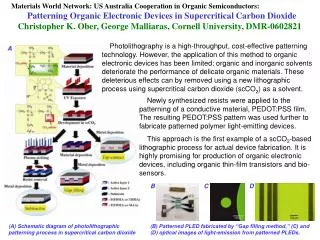
Materials World Network: US Australia Cooperation in Organic Semiconductors: Patterning Organic Electronic Devices in Supercritical Carbon DioxideChristopher K. Ober, George Malliaras, Cornell University, DMR-0602821 Photolithography is a high-throughput, cost-effective patterning technology. However, the application of this method to organic electronic devices has been limited; organic and inorganic solvents deteriorate the performance of delicate organic materials. These deleterious effects can by removed using a new lithographic process using supercritical carbon dioxide (scCO2) as a solvent. A Newly synthesized resists were applied to the patterning of a conductive material, PEDOT:PSS film. The resulting PEDOT:PSS pattern was used further to fabricate patterned polymer light-emitting devices. This approach is the first example of a scCO2-based lithographic process for actual device fabrication. It is highly promising for production of organic electronic devices, including organic thin-film transistors and bio-sensors. B C D (A) Schematic diagram of photolithographic patterning process in supercritical carbon dioxide (B) Patterned PLED fabricated by “Gap filling method,” (C) and (D) optical images of light-emission from patterned PLEDs.
Development of Perfluoroalkylated Light-Emitting PolyfluorenesChristopher K. Ober, George Malliaras, Cornell University, DMR-0602821 Education: As part of our collaboration with Prof. Andrew Holmes at University of Melbourne (Australia), J. K. Lee visited Australia (March 2007) and graduate student Ms. Georgia McCluskey visited the Ober group (June 2007) to further extend research ideas. Undergraduate researchers at Cornell are active participants of this program. Each summer the PI hosts ~5 REU students, each working under a mentor. • Outreach: • The PIs take part in Cornell University organized science teachers workshops. In addition, the PIs visit local high schools to discuss polymer science and new developments in nanotechnology. • Ober co-organized IUMACRO-07, held in New York City, a IUPAC sponsored international conference. The PI’s group members were all able to present their work and to interact with many outstanding scientists. • For the last 6 months, Ober has been organizing an NSF-sponsored two-day workshop on Research and Education Opportunities In Interdisciplinary, Globally Leading Polymer Science And Engineering held August 2007. Ober research group with Robert Lenz on the occasion of his Biopolymer Award at IUMACRO-07 Student poster session at IUMACRO-07