
Memory Definitions
E N D
Presentation Transcript
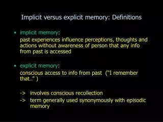
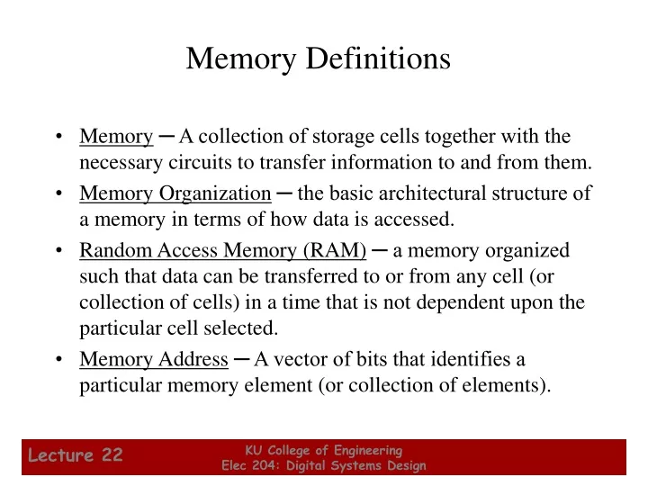
Memory Definitions • Memory ─ A collection of storage cells together with the necessary circuits to transfer information to and from them. • Memory Organization ─ the basic architectural structure of a memory in terms of how data is accessed. • Random Access Memory (RAM) ─ a memory organized such that data can be transferred to or from any cell (or collection of cells) in a time that is not dependent upon the particular cell selected. • Memory Address ─ A vector of bits that identifies a particular memory element (or collection of elements). KU College of Engineering Elec 204: Digital Systems Design
Memory Definitions (Continued) • Typical data elements are: • bit ─ a single binary digit • byte ─ a collection of eight bits accessed together • word ─ a collection of binary bits whose size is a typical unit of access for the memory. It is typically a power of two multiple of bytes (e.g., 1 byte, 2 bytes, 4 bytes, 8 bytes, etc.) • Memory Data ─ a bit or a collection of bits to be stored into or accessed from memory cells. • MemoryOperations ─ operations on memory data supported by the memory unit. Typically, read and write operations over some data element (bit, byte, word, etc.). KU College of Engineering Elec 204: Digital Systems Design
Memory Organization • Organized as an indexed array of words. Value of the index for each word is the memory address. • Often organized to fit the needs of a particular computer architecture. Some historically significant computer architectures and their associated memory organization: • Digital Equipment Corporation PDP-8 – used a 12-bit address to address 4096 12-bit words. • IBM 360 – used a 24-bit address to address 16,777,216 8-bit bytes, or 4,194,304 32-bit words. • Intel 8080 – (8-bit predecessor to the 8086 and the current Intel processors) used a 16-bit address to address 65,536 8-bit bytes. KU College of Engineering Elec 204: Digital Systems Design
n Data Input Lines n Memory k Address Lines Unit k 2k Words n Bits per Word 1 Read 1 Write n n Data Output Lines Memory Block Diagram • A basic memory system is shown here: • k address lines are decoded to address 2k words of memory. • Each word is n bits. • Read and Write are single control lines defining the simplest of memory operations. KU College of Engineering Elec 204: Digital Systems Design
Memory Address Memory Binary Decimal Content 0 0 0 0 1 0 0 0 1 1 1 1 0 0 1 1 1 1 1 1 1 1 1 1 0 1 0 2 1 0 1 1 0 0 0 1 0 1 1 3 0 0 0 0 0 0 0 0 1 0 0 4 1 0 1 1 1 0 0 1 1 0 1 5 1 0 0 0 0 1 1 0 1 1 0 6 0 0 1 1 0 0 1 1 1 1 1 7 1 1 0 0 1 1 0 0 Memory Organization Example • Example memory contents: • A memory with 3 address bits & 8 data bits has: • k = 3 and n = 8 so 23 = 8 addresses labeled 0 to 7. • 23 = 8 words of 8-bit data KU College of Engineering Elec 204: Digital Systems Design
Basic Memory Operations • Memory operations require the following: • Data ─ data written to, or read from, memory as required by the operation. • Address ─ specifies the memory location to operate on. The address lines carry this information into the memory. Typically: n bits specify locations of 2n words. • An operation ─ Information sent to the memory and interpreted as control information which specifies the type of operation to be performed. Typical operations are READ and WRITE. Others are READ followed by WRITE and a variety of operations associated with delivering blocks of data. Operation signals may also specify timing info. KU College of Engineering Elec 204: Digital Systems Design
Basic Memory Operations (continued) • Read Memory─ an operation that reads a data value stored in memory: • Place a valid address on the address lines. • Wait for the read data to become stable. • Write Memory─ an operation that writes a data value to memory: • Place a valid address on the address lines and valid data on the data lines. • Toggle the memory write control line • Sometimes the read or write enable line is defined as a clock with precise timing information (e.g. Read Clock, Write Strobe). • Otherwise, it is just an interface signal. • Sometimes memory must acknowledge that it has completed the operation. KU College of Engineering Elec 204: Digital Systems Design
Memory Operation Timing • Most basic memories are asynchronous • Storage in latches or storage of electrical charge • No clock • Controlled by control inputs and address • Timing of signal changes and data observation is critical to the operation • Read timing: 20 ns Clock T1 T2 T3 T4 T1 Address Address valid Memory enable Read/ Write Data Data valid output 65 ns Read cycle KU College of Engineering Elec 204: Digital Systems Design
Memory Operation Timing 20 ns T1 T2 T3 T4 T1 Clock • Write timing: • Critical times measured with respect to edges of write pulse (1-0-1): • Address must be established at least a specified time before 1-0 and held for at least a specified time after 0-1 to avoid disturbing stored contents of other addresses • Data must be established at least a specified time before 0-1 and held for at least a specified time after 0-1 to write correctly Address valid Address Memory enable Read/ Write Data Data valid input 75 ns Write cycle KU College of Engineering Elec 204: Digital Systems Design
RAM Integrated Circuits • Types of random access memory • Static – information stored in latches • Dynamic – information stored as electrical charges on capacitors • Charge “leaks” off • Periodic refresh of charge required • Dependence on Power Supply • Volatile – loses stored information when power turned off • Non-volatile – retains information when power turned off KU College of Engineering Elec 204: Digital Systems Design
Static RAM Cell Select • Array of storage cells used to implement static RAM • Storage Cell • SR Latch • Select input forcontrol • Dual Rail DataInputs B and B • Dual Rail DataOutputs C and C B C S Q C R Q B RAM cell KU College of Engineering Elec 204: Digital Systems Design
Static RAM Bit Slice Select Word select 0 B C X S Q • Represents all circuitry that is required for 2n 1-bit words • Multiple RAM cells • Control Lines: • Word select i– one for each word • Bit Select • Data Lines: • Data in • Data out Word C X select R Q B 0 RAM cell RAM cell Word select 1 RAM cell Select Word select n 2 1 Word X S Q select n 1 2 RAM cell X R Q RAM cell Read/Write logic Data in Q Data out S Data in Read/ Bit Write select R Q Write logic Data out Read logic Bit Read/ select Write KU College of Engineering Elec 204: Digital Systems Design
2n-Word 1-Bit RAM IC Word select 4-to-16 0 Decoder 3 A A 1 2 3 3 2 RAM cell 2 A A 3 2 2 2 4 1 A A 5 2 1 1 • To build a RAM ICfrom a RAM slice,we need: • Decoder decodesthe n address lines to2n word select lines • A 3-state buffer • on the data outputpermits RAM ICs tobe combined into aRAM with c 2n words 6 RAM cel l 0 7 A A 2 0 0 16 x 1 8 RAM 9 10 11 Data Data output input 12 13 14 15 Read/ Write RAM cell Memory enable Read/Write (a) Symbol logic Data input Data in Data out Read/ Bit Write select Data output Read/Write Chip select (b) Block diagram KU College of Engineering Elec 204: Digital Systems Design
Cell Arrays and Coincident Selection • Memory arrays can be very large => • Large decoders • Large fanouts for the bit lines • The decoder size and fanouts can be reduced by approximately by using a coincident selection ina 2-dimensional array • Uses two decoders, one for words and one for bits • Word select becomes Row select • Bit select becomes Column select • See next slide for example • A3 and A2 used for Row select • A1 and A0 for Column select KU College of Engineering Elec 204: Digital Systems Design
Row decoder Cell Arrays and Coincident Selection 2-to-4 Decoder 0 1 A 2 3 RAM cell RAM cell RAM cell RAM cell 0 1 2 3 0 A 2 2 1 RAM cell RAM cell RAM cell RAM cell Row 4 5 6 7 select 2 RAM cell RAM cell RAM cell RAM cell 8 9 10 11 3 RAM cell RAM cell RAM cell RAM cell 12 13 14 15 Read/Write Read/Write Read/Write Read/Write logic logic logic logic Data in Data in Data in Data in Data out Data out Data out Data out Read/ Bit Read/ Bit Read/ Bit Read/ Bit Write select Write select Write select Write select Data input Read/Write X X X X Column select Data output 0 1 2 3 Column 2-to-4 Decoder decoder with enable 1 0 2 2 Enable A A 1 0 Chip select KU College of Engineering Elec 204: Digital Systems Design
Making Larger Memories • Using the CS lines, we can make larger memories from smaller ones by tying all address, data, and R/W lines in parallel, and using the decoded higher order address bits to control CS. • Using the 4-Word by 1-Bit memory from before, we construct a 16-Word by1-Bit memory. KU College of Engineering Elec 204: Digital Systems Design
Making Wider Memories • To construct wider memories from narrow ones, we tie the address and control lines in parallel and keep the data lines separate. • For example, to make a 4-word by 4-bit memory from 4, 4-word by 1-bit memories • Note: Both 16x1 and 4x4 memories take 4-chips and hold 16 bits of data. KU College of Engineering Elec 204: Digital Systems Design