Forward Multiplicity Detector (status and progress)
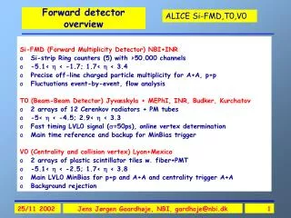
Forward Multiplicity Detector (status and progress). Si-FMD (Forward Multiplicity Detector) Si-strip Ring counters (5) with 50.000 channels -5.1< < -1.7; 1.7< < 3.4 Off-line charged particle multiplicity for A+A, p+p Fluctuations event-by-event, flow analysis


Forward Multiplicity Detector (status and progress)
E N D
Presentation Transcript
Forward Multiplicity Detector (status and progress) Si-FMD (Forward Multiplicity Detector) • Si-strip Ring counters (5) with 50.000 channels • -5.1< < -1.7; 1.7< < 3.4 • Off-line charged particle multiplicity for A+A, p+p • Fluctuations event-by-event, flow analysis • Geometry and integration defined.Prototyping of mech. Supports. • Final Si-sensor design ongoing. • Read out chain (FEE-BEE-DAQ) defined.Prototyping ongoing. • Performance/simulations • TDR in preparation. • Concerns: ’ambient’ temperature, material Jens Jørgen Gaardhøje, NBI, gardhoje@nbi.dk
Si-FMD Si1 Si2 Si3 • 5 Si-strip rings segmented into 50.000 channels • Rapidity coverage from ITS (1.7) to 5.1. • Segmentation sufficient for ‘Poisson’ analysis • Main Off-line charged particle multiplicity studies • Average multiplicity (entropy, stopping) • Fluctuations (phase transitions) • Flow (thermalisation, hydrodynamics) Jens Jørgen Gaardhøje, NBI, gardhoje@nbi.dk
pp Forward rapidity physics at LHC BRAHMS@ RHIC snn= 200AGeV Plateau at LHC –6<<+6 ? Jens Jørgen Gaardhøje, NBI, gardhoje@nbi.dk
CERN Maquette 1:1 ITS-pixels V0-R T0-R Si1(outer) Si1 (inner) Absorber Jens Jørgen Gaardhøje, NBI, gardhoje@nbi.dk
Mechanical Installation Jens Jørgen Gaardhøje, NBI, gardhoje@nbi.dk
FMD Cabling on muon side Digitized signals , HV and control Jens Jørgen Gaardhøje, NBI, gardhoje@nbi.dk
Si1 mechanics model 1:1 Outer ring not shown Beam pipe support ring Si detectors Support plate Engineering study in progress to minimize material, maximize rigidity Digitizer card Jens Jørgen Gaardhøje, NBI, gardhoje@nbi.dk
Heat dissipation • Heat dissipated by FE electronics of one Si detector ring: VA1’’ preamp chip (128 channels): 235 mW 80 chips = 19 W / ring Read-out electronics and power distribution: 5 W/ring Cooling: air flow between Si detector and support plate radiation from VA chips to support. active (water) cooling of support plate is considered Detailed cooling studies (simulations of heat profile) need to be done. Presently, the temperature at the FMD, T0, V0 location is >70 deg. due to ITS heat dissipation. Effective general cooling of this region required ! Jens Jørgen Gaardhøje, NBI, gardhoje@nbi.dk
Left Side: Si2 & Si3 Details of mounting to be finalized Jens Jørgen Gaardhøje, NBI, gardhoje@nbi.dk
Si rings manufactured of 6” wafers Inner: Rin=4.2 cm Rout=17.2 cm Outer: Rin=15.4 cm Rout=28.4 cm 256 Possible suppliers: Micron, UK Hamamatsu, JP 512 10x2x512=10240 20x2x256=10240 Jens Jørgen Gaardhøje, NBI, gardhoje@nbi.dk
Coverage in pseudorapidity Design criteria: Largest possible coverage Largest symmetry left and right Overlap between systems Constraints: Vacuum tube outer envelope: 42 mm, Outer radius, ITS, Absorber, cables Background from secondaries(small angles) Si1: Out: 1.70< <2.29In: 2.01< <3.40 Si2: Out: -2.29<<-1.7 In: -3.68< <-2.28 Si3: In: -5.09< <-3.68 Vertex shift (10cm): |d| 0.1 Jens Jørgen Gaardhøje, NBI, gardhoje@nbi.dk
Details of Si sensors Hamamatsu, Micron Jens Jørgen Gaardhøje, NBI, gardhoje@nbi.dk
Adjusted acceptance Jens Jørgen Gaardhøje, NBI, gardhoje@nbi.dk
Hybrid with Viking PA chips Connector(s) for power, control, read-out • Hybrid cards contain: • FE–Preampl. chips • Bias voltages distribution • Gate/strobe distribution • Read-out clock distribution • Detector bias connection Other components VA preamp+shaper: 128 ch Si detector Jens Jørgen Gaardhøje, NBI, gardhoje@nbi.dk
FMD Read-Out and Control Electronics IN COUNTING ROOM ON DETECTOR IN CAVERN FMD Segment Digital serial links (15-20 m) Analog serial link (10 MHz) 0.5 m FMD RCU Detector Data Link (50-60 m) FMD Digitizer ALTRO CTRL Data receiver DDL - INT ALTRO CTRL BOARD ALTRO CTRL CTRL Interface Slow-Control Controller Slow control & Trigger Local TTC-RX Read-out CTRL VA read-out control Trigger & Slow Ctrl VA 1 ring: 10/20 segments 2 Digitizers 1 RCU per side 1 DDL per side Full FMD: 70 segments 10 Digitizers 2 RCU’s 2 DDL’s BSN, 21 Nov 2002 FMD RO strategy Jens Jørgen Gaardhøje, NBI, gardhoje@nbi.dk
Si-FMD electronics overview SI-FMD channel count Note: We have increased the number of strips, but use more integrated FE chips – red values are changed. Jens Jørgen Gaardhøje, NBI, gardhoje@nbi.dk
FMD FEE test Ext trigger ALTRO tester CTRL Ext clock ALTRO Power Biases Clock 10 MHz Si detector VA CTRL Trig in BSN, 21 Nov 2002 FMD FEE test setup Labview DAQ • NBI test board: • generates trigger • + pulse on Si det • level adaption of • VA-to-ALTRO • VA read-out clock • + controls • ALTRO digitization • clock (sync.) Jens Jørgen Gaardhøje, NBI, gardhoje@nbi.dk
Si-FEE-Digitizer prototyping at NBI DAQ/ Labview Si-strip detector + VA’’ preamp VA’’ read-out controller ALTRO tester Jens Jørgen Gaardhøje, NBI, gardhoje@nbi.dk
First prototype test results Output from VA chip: (128 channels multiplexed into serial read-out) Note: 3 bad Si/VA channels Output from ALTRO: (128 time bins are digitized) Note: general shape + 3 bad channels repeated Noise still too high Timing still not stable Si+ Preamp Out Trigger Altro Out Jens Jørgen Gaardhøje, NBI, gardhoje@nbi.dk
FMD 28/02/03 [FSM?] Database(s) Control room (ACR) PVSS II PVSS II PVSS II OPCclient DIMclient User interface Ethernet PVSS II PVSS II PVSS II OPS client OPC client OPC client CAEN OPCserver CAEN OPCserver DIMserver ? PCI-CAN? PCI-CAN? PCI-Profibus PCI-CAN? E E P C Ethernet is considered as alternative CAEN ? CAEN ? DDL TTC FMD-RCU (PCI? VME?) P? LVL0 trig 10 1 2 1 HV LV LV 300? 20 140 10 2 70 Detector Preamps FMD Digitizers Digitizers High Voltage Preamps Crate Control Slow ControlsFollow main strategy DCS Counting room Cavern In magnet Jens Jørgen Gaardhøje, NBI, gardhoje@nbi.dk
Charged particle occupancy including secondaries Si-1 outer Si-3 x 2 x 2 x 2 Si-1 inner 1 1 1 20 sectors 512 strips each 10240 channels 40 sectors 256 strips each 10240 channels 20 sectors 512 strips each 10240 channels Have increased number of strips by factor of 2 using ’128 ch VA-prime’ PA chip at practically same cost => average occupancy <1 for most strips! Jens Jørgen Gaardhøje, NBI, gardhoje@nbi.dk
Background from Secondaries Si2 inner Si1 inner Si1 outer Si3 Primaries Beam pipe ITS T0,V0,Abs, frames Jens Jørgen Gaardhøje, NBI, gardhoje@nbi.dk
Reconstruction of ’true’ multiplicity 1 HIJING event 10 HIJING events Input dist and reconstructed Primaries+secondaries Primaries HijingGeant= R * Hijing R = R() response matrix Jens Jørgen Gaardhøje, NBI, gardhoje@nbi.dk
Iterative convolution of trial spectrum O = R * TrueSpec O(0)= R(0)* H TrueSpec(1)=O/O(1)*H O(1)= R(1)* TrueSpec(1) …Continue until O(n)O Test of flat input distribution Jens Jørgen Gaardhøje, NBI, gardhoje@nbi.dk
Si-FMD timetable (1) Jens Jørgen Gaardhøje, NBI, gardhoje@nbi.dk
Si-FMD timetable (2) Pre-assembly test July-Nov 2004 Construction, assembly , test at RHIC 2005 Installation June-Sept 2006 Jens Jørgen Gaardhøje, NBI, gardhoje@nbi.dk
Si-FMD, TO,VOTDR time table. • Fair amount of written material exists already (T0 100 pgs, Si-FMD 50 pgs, V0 20 pgs) • April 15. Collect first detector chapters. • June ’03. Editorial meeting. 1rst draft. • Summer ’03 Si-FMD electronics chain test. • June ’03 T0 test beam • August ’03 V0 test beam • TDR writing: fall 2003 Jens Jørgen Gaardhøje, NBI, gardhoje@nbi.dk
Techical Design Report Alice collab list. (5pgs) Summary of contents (2pgs) Table of contents. List of tables and figs. (4pgs) Color pictures of selected det. elements etc. (6pgs) 1. Physics objectives and design considerations T0, V0, Si-FMD trigger, timing, on-line mult, off-line mult, fluct, bgd rejection, overall performance, coverage etc ... (10 pgs) 2. Design objectives, mechanical structure, Integration T0, V0, Si-FMD mounting, tolerances, clearances, inst. seq., cooling, cabling ... (10pgs) 3. T0 (40 pgs) 4. V0 (40 pgs) 5. Si-FMD (40 pgs) 6. Installation, slow control, DAQ, safety. (10 pgs) 7. Organization (5 pgs) Group org., construction, installation, cost 8. References. (4pgs) 9. Index (2 pgs) (approx. 180 pgs) Jens Jørgen Gaardhøje, NBI, gardhoje@nbi.dk
Tasks and decisionsfor Weekly meetings (1) 1) Si sensors: - define final specs of sensor properties - negotiate price again with Hamamatsu and Micron - choose company - order prototype 2) Voltage supplies - define Voltage requirements (Volt, current, remote control and DCS) - investigate market (check out ITS or other Si systems in ALICE) 3) Bonding - decide on bonding strategy (CERN or other) - make arrangement with bonder 4) FEE-preamplifier card. - define final specs of FEE hybrid card - define interface to ALTRO -digitizer card and other slow controls. - define strategy: home built hybrid card with VA-prime from IDEAS or design and production by IDEAS and production for card? -updated cost estimate for industrial design and production (IDEAS) Jens Jørgen Gaardhøje, NBI, gardhoje@nbi.dk
Tasks and decisionsfor Weekly meetings(2) 5) Digitizer card (ALTRO board) -define interface to FEE and RCU - define necessary modifications to standard ALTRO boards 6) RCU card. - define interface to digitizer card (ALTRO board) - define necesary modifications to RCU 7) DDL and connection to DAQ -define modifications needed, if any 8) cabling and services, cooling - define cable types and length. - define connectors - define own cooling needs - define placement of cards/DDL etc in ALICE 9) Mechanical - define mechanical mounts for Si1, Si2, Si3. 10) Slow Control and DAQ communication - define tasks to be done -collect information and establish contact with DCS and DAQ groups. Jens Jørgen Gaardhøje, NBI, gardhoje@nbi.dk
Extra’s Jens Jørgen Gaardhøje, NBI, gardhoje@nbi.dk
Front end electronics REQUIREMENTS: Adapted for 5-25pF capacitance (300m Si, 0.5 cm2: 25pF, 1MIP: 22.400 e-) Dynamic range: 0-20 MIPS Radiation hardness: >200kRad Peaking time: 1-2 s Low noise (good S/N) High integration Sample/hold and serial read-out, 10 MHz clock Moderate power consumption Simple slow controls and power reg. Affordable cost VA1 prime 2 (Viking-IDEAS): Input capacitance: < 30 pF 0-20 MIPs >1MRad (0.35 m tech.) 1-3 s 475 e- at 25 pF => S/N 20:1 128 10 Mhz clock 1.3 mW/ch Test system available OK Jens Jørgen Gaardhøje, NBI, gardhoje@nbi.dk
Multiplicity resolution Jens Jørgen Gaardhøje, NBI, gardhoje@nbi.dk
Reconstructed multiplicity.Average and width 1.7 Background Subtracted All hits reconstructed 3.4 Jens Jørgen Gaardhøje, NBI, gardhoje@nbi.dk
Background Si2outer Si2inner Si1outer Si3 Si1inner h=1.73 h=2.4 h=1.31 Jens Jørgen Gaardhøje, NBI, gardhoje@nbi.dk Alla Maevskaia ALICE Week 9 September 2003