Exploring the Quantum Vacuum: Casimir Effect and MIR Experiment
390 likes | 421 Vues
Discover the fascinating effects of the quantum vacuum at microscopic and macroscopic levels, including the groundbreaking Casimir effect. Learn about the theoretical foundations, experimental verifications, and future possibilities such as the MIR experiment proposal. Dive into the significance of parametric resonance conditions, amplification techniques, and the potential for dynamic Casimir effects through innovative approaches. Join the scientific exploration of the quantum vacuum's intricacies and its implications on modern physics.

Exploring the Quantum Vacuum: Casimir Effect and MIR Experiment
E N D
Presentation Transcript
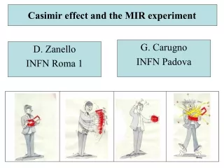
G. Carugno INFN Padova Casimir effect and the MIR experiment D. Zanello INFN Roma 1
The quantum vacuum and its microscopic consequences The static Casimir effect: theory and experiments Friction effects of the vacuum and the dynamical Casimir effect The MIR experiment proposal Summary
Quantum vacuum is not empty but is defined as the minimun of the energy of any field Its effects are several at microscopic level: Lamb shift Landè factor (g-2) Mean life of an isolated atom The quantum vacuum
The static Casimir effect • This is a macroscopic effect of the quantum vacuum, connected to vacuum geometrical confinement • HBG Casimir 1948: the force between two conducting parallel plates of area S spaced by d
Experimental verifications • The first significant experiments were carried on in a sphere-plane configuration. The relevant formula is R is the sphere radius
Results of the Padova experiment (2002) First measurement of the Casimir effect between parallel metallic surfaces
Fulling and Davies (1976): effects of the vacuum on a moving mirror Steady motion (Lorentz invariance) Uniformly accelerated motion (Free falling lift) Non uniform acceleration (Friction!): too weak to be detectable Friction effects of the vacuum Nph ~ W T (v/c)2
GT Moore (1970): proposes the use of an RF EM cavity for photon production Dodonov et al (1989), Law (1994), Jaeckel et al (1992): pointed out the importance of parametric resonance condition in order to multiply the effect Amplification using an RF cavity wm = excitation frequency w0 = cavity resonance frequency wm = 2 w0
The parametric resonance is a known concept both in mathematics and physics In mathematics it comes from the Mathieu equations In physics it is known in mechanics (variable length swing) and in electronics (oscillating circuit with variable capacitor) Parametric resonance
Theoretical predictions • Linear growth A.Lambrecht, M.-T. Jaekel, and S. Reynaud, Phys. Rev. Lett. 77, 615 (1996) 2. Exponential growth V. Dodonov, et al Phys. Lett. A 317, 378 (2003); M. Crocce, et al Phys. Rev. A 70, (2004); M. Uhlmann et alPhys. Rev. Lett. 93, 19 (2004) t is the excitation time
Is energy conserved? Eout Eout E E Ein Ein Eout t t Srivastava (2005):
Resonant RF Cavity In a realistic set-up a 3-dim cavity has an oscillating wall. Wm Cavity with dimensions ~ 1 -100 cm have resonance frequency varying from 30 GHz to 300 MHz. (microwave cavity) Great experimental challenge: motion of a surface at frequencies extremely large to match cavity resonance and with large velocity (b=v/c)
Mechanical motion. Strong limitation for a moving layer: INERTIA Very inefficient technique: to move the electrons giving the reflectivity one has to move also the nuclei with large waste of energy Maximum displacement obtained up to date of the order of 1 nm Effective motion. Realize a time variable mirror with driven reflectivity (Yablonovitch (1989) and Lozovik (1995) Surface motion
Time variable mirror Resonant cavity with time variable mirror MIR Experiment
The Project Dino ZanelloRome Caterina BraggioPadova Gianni Carugno Giuseppe Messineo Trieste Federico Della Valle Giacomo BressiPavia Antonio Agnesi Federico Pirzio Alessandra Tomaselli Giancarlo Reali Giuseppe Galeazzi LegnaroLabs Giuseppe Ruoso MIR – RD 2004-2005 R & D financed by National Institute for Nuclear Physics (INFN) MIR 2006 APPROVED AS Experiment.
Time variable mirror Our approach Taking inspiration from proposals by Lozovik (1995) and Yablonovitch (1989) we produce the boundary change by light illumination of a semiconductor slab placed on a cavity wall Semiconductors under illumination can change their dielectric properties and become from completely transparentto completely reflective for selected wavelentgh. A train of laser pulses will produce a frequency controlled variable mirror and thus if the change of the boundary conditions fulfill the parametric resonance condition this will result in the Dynamical Casimir effect with the combined presence of high frequency, large Q and large velocity
Expected results Complete characterization of the experimental apparatus has been done by V. Dodonov et al (see talk in QFEXT07). V V Dodonov and A V Dodonov “QED effects in a cavity with time-dependent thin semiconductor slab excited by laser pulses” J Phys B 39 (2006) 1-18 Calculation based on realistic experimental conditions, • t semiconductor recombination time , 10-30 ps • semiconductor mobility , 1 m 2 / (V s) • () semiconductor light absorption coefficient • t semiconductor thickness , t 1 mm • laser: 1 ps pulse duration, 200 ps periodicity, 10-4 J/pulse • (a, b, L) cavity dimensions Expected photons N > 103 per train of shots
Photon generation plus damping A0 = 10 D = 2 mm = b = 3 104 cm2/Vs = 2.5 GHz = 12 cm (b = 7 cm, L = 11.6)
Measurement set-up Cryostat wall The complete set-up is divided into Laser system Resonant cavity with semiconductor Receiver chain Data acquisition and general timing
Experimental issues • Effective mirror • the semiconductor when illuminated behaves as a metal (in the microwave band) • timing of the generation and recombination processes • quality factor of the cavity with inserted semiconductor • possible noise coming from generation/recombination of carriers • Laser system • possibility of high frequency switching • pulse energy for complete reflectivity • number of consecutive pulses • Detection system • minimum detectable signal • noise from blackbody radiation
Semiconductor as a reflector Reflection curves for Si and Cu Light pulse Experimental set-up • Results: • Perfect reflectivity for microwave Si, GaAs: R=1; • Light energy to make a good mirror ≈ 1 mJ/cm2 Time (ms)
Semiconductor I The search for the right semiconductor was very long and stressful, but we managed to find the right material Requests: t ~ 10 ps , m ~ 1 m2/ (V s) Neutron Irradiated GaAs Irradiation is done with fast neutrons (MeV) with a dose ~ 1015 neutrons/cm2 (performed by a group at ENEA - ROMA). These process while keeping a high mobility decreases the recombination time in the semiconductor High sensitivity measurements of the recombination time performed on our samples with the THzpump and probe technique by the group of Prof. Krotkus in Vilnius (Lithuania)
Semiconductor II: recombination time Results obtained from the Vilnius group on Neutron Irradiated GaAs Different doses and at different temperatures The technique allows to measure the reflectivity from which one calculate the recombination time 1. Same temperature T = 85 K 2. Same dose (7.5E14 N/cm2) Estimated t = 18 ps
Semiconductor III: mobility Mobility can be roughly estimated for comparison with a known sample from the previous measurements and from values of non irradiated samples. m ~ 1 m2 / (V s) We are setting up an apparatus for measuring the product mt using the Hall effect. From literature one finds that little change is expected between irradiated and non irradiated samples at our dose
Cavity with semiconductor wall Fundamental mode TE101: the electric field E Computer model of a cavity with a semiconductor wafer on a wall a = 7.2 cm b = 2.2 cm l = 11.2 cm QL= measured ≈3· 106 600 m thick slab of GaAs
Cryostats old new Superconducting cavity Cavity geometry and size optimized after Dodonov’s calculations Niobium: 8 x 9 x 1 cm3 Semiconductor holding top Antenna hole Q value ~ 107 for the TE101 mode resonant @ 2.5 GHz No changes in Q due to the presence of the semiconductor The new one has a 50 l LHe vessel Working temperature 1 - 8 K
(Cryogenic) Electronics I Final goal is to measure about 103 photons @ 2.5 GHz Use a very low noise cryogenic amplifier and then a superheterodyne detection chain at room temperature Picture of the room temperature chain The cryogenic amplifier CA has 37 dB gain allowing to neglect noise coming from the rest of the detector chain Special care has to be taken in the cooling of the amplifier CA and of the cable connecting the cavity antenna to it CA PA
Electronics II: measurements Motorized control of the pick-up antenna Superconducting cavity ~ 10 cm Cryogenic amplifier
Electronics III: noise measurement Using a heated 50 W resistor it is possible to obtain noise temperature of the first amplifier and the total gain of the receiver chain 2. Complete chain 1. Amplifier + PostAmplifier
Sensitivity The power P measured by the FFT is: kB - Boltmann’s constant G - total gain B - bandwidth TN - amplifier noise temperature TR - 50 W real temperature Results: TN1 = TN2 No extra noise added in the room temperature chain G1 = 72 dB = 1.6 107 Gtot = 128 dB = 6.3 1012 The noise temperature TN = 7.2 K corresponds to 1 10-22 J For a photon energy = 1.7 10-24 J sensitivity ~ 100 photons
Black Body Photons in Cavity at Resonance Noise 50 Ohm Resistor at R.T. Noise Signal from TE101 Cavity at R.T. Cavity Noise vs Temperature
Laser system I Pulsed laser with rep rate ~ 5 GHz, pulse energy ~100 mJ, train of 103 - 104 pulses, slightly frequency tunable ~ 800 nm Laser master oscillator 5 GHz, low power Pulsepicker Optical amplifier Total number of pulses limited by the energy available in the optical amplifier Each train repeated every few seconds Optics Express 13, 5302 (2005)
Laser system II Diode preamplifier Master oscillator Pulse picker Current working frequency: 4.73 GHz Pulse picker: ~ 2500 pulses, adjustable Diode preamplifier gain: 60 dB Final amplifier gain: > 20 dB Total energy of the final bunch: > 100 mJ Flash lamp final amplifier
Detection scheme Steps Find cavity frequency nr Wait for empty cavity Set laser system to 2 nr Send burst with > 1000 pulses Look for signal witht ~ Q / 2pnr Expected number of photons: Niobium cavity with TE101nr = 2.5 GHz (22 x 71 x 110 mm3) Semiconductor GaAs with thickness dx = 1 mm Single run with ~ 5000 pulses N ≥ 103 photons
Check list Several things can be employed to disentangle a real signal from a spurious one Loading of cavity with real photons (is our system a microwave amplifier?) Change temperature of cavity Effect on black body photons Change laser pulse rep. frequency • change recombination time of semiconductor • change width of semiconductor layer
Carry on measurements at different temperatures and extrapolate to T = 0 Kelvin Loading of cavity with real photons and measure Gain Change laser pulse rep. frequency Conclusions Several things can be employed to disentangle a real signal from a spurious one We expect to complete assembly Spring this year. First measure is to test the amplification process with preloaded cavity, then vacuum measurements • change recombination time of semiconductor • change thickness of semiconductor
Frequency shift Problem: derivation of a formula for the shift of resonance in the MIR em cavity and compare it with numerical calculations and experimental data. 0 -L complex dielectric function transparent background G D Result: a thin film is an ideal mirror (freq shift) even if G s MIR experiment: 800 nm light impinging on GaAs + 1 m abs. Length = plasma thickness + mobility 104 cm2/Vs mcm A>1
Nb = n = T/2 • Nph = sinh2(n) = sinh2(T0) ideal case • unphysically large number of photons • dissipation effects (instability removed) • T 0 non zero temperature experiment? Nph = sinh2(n)(1+2 <N1>0) thermal photons are amplified as well
Surface effective motion II Generate periodic motion by placing the reflecting surface in two distinct positions alternatively Position 1 - metallic plate Position 2 - microwave mirror with driven reflectivity USE Semiconductors under illumination can change their dielectric properties and become from completely transparent to completely reflective for microwaves. Light with photon energy hn > E band gap of semiconductor Enhances electron density in the conduction band Laser ON - OFF On semiconductor Time variable mirror