Download
1 / 10
100 likes | 205 Vues
An overview of a high-speed data processing system for particle detection, featuring advanced modularity and 9U VME64x form factor. Includes Opto Links, Front-End Modules, Back-End modules, and various interfaces for effective control and monitoring. History of FEDv1 manufacture and testing, along with development of FEDv2 hardware changes, firmware, and FPGA configurations. Outlines production plans and schedule for FEDv2.

E N D
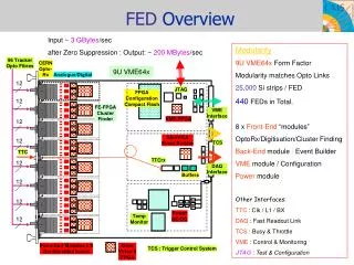
12 12 12 12 12 12 12 12 FED Overview Input ~ 3 GBytes/sec after Zero Suppression : Output: ~ 200 MBytes/sec Modularity 9U VME64x Form Factor Modularity matches Opto Links 25,000 Si strips / FED 440 FEDs in Total. 8 x Front-End “modules” OptoRx/Digitisation/Cluster Finding Back-Endmodule / Event Builder VME module / Configuration Power module Other Interfaces: TTC : Clk / L1 / BX DAQ : Fast Readout Link TCS : Busy & Throttle VME : Control & Monitoring JTAG : Test & Configuration 96 Tracker Opto Fibres CERN Opto- Rx 9U VME64x Analogue/Digital JTAG FPGA Configuration Compact Flash FE-FPGA Cluster Finder VME Interface VME-FPGA BE-FPGA Event Builder TCS TTC TTCrx DAQ Interface Buffers Power DC-DC Temp Monitor Front-End Modules x 8 Double-sided board Xilinx Virtex-II FPGA TCS : Trigger Control System
FEDv1 9U Board • 9U VME64x • PCB 14 layers (incl 6 power & ground) • ~ 6 K components (smallest 0402) ; ~ 25 K tracks • BGAs largest 676 pins @ 1 mm pitch • 96 ADC channels : • AD9218 Dual package 10 bit @ 40 MHz • Half Analogue circuitry on Secondary Side • JTAG Boundary Scan • 6 FEDv1 boards delivered to CERN for Large Scale Assembly centres (4 used in 25 nsec test beam June 2004) • 5 FEDv1 boards kept in UK for Design Tests
FEDv1 Manufacture History Sep 2003 • 5 FEDv1 boards under test. (PCB and Assembly done by separate small companies) All boards working well. Only manufacturing minor faults. Oct 2003 • Further 6 FEDv1 made. (same manufacturers) Major problems on all boards. Shorts under many BGAs. Rework of BGAs attempted. After initial success on 2 boards failed on next 4. Problem believed due to uncured solder resist ink leeching from vias of bare PCBs. Diagnosis complicated by split manufacture and change from Ni/Gold to Immersion Tin metal finish. Nov 2003 - Jan 2004 Identified candidate medium size companies suitable for 500 production boards. Providing combined PCB and Assembly with guarantees. Offering advanced Quality Controls, Auto Optical Inspection, X-ray (in house), BScan. Mar 2004 • Manufactured 6 FEDv1 with one of the identified companies. Very professional production process. No BGA problems. All boards working well.
FEDv1 Design Testing Hardware • Design verified @ 100 kHz L1. • S-LINK readout @ 80 MHz. • Analogue circuits characterised. Optical inputs using FED Opto-Tester board. Switch to operate ADC in 1V pp mode (due to ADC bug). Minor mod on FED. To match new OptoRx some FED FE component values will need tuning. • Interfaces to TTC and TCS verified. • FED power/temp requirements finalised. Standard LHC crates satisfactory. Firmware • Baseline design working, used in 25 nsec Test Beams June 2004. • Some readout errors in Zero Suppression mode. Under investigation. • Software • FED is fully integrated in CMS Tracker DAQ framework. • Test bench Framework for essential Assembly Plant Testing nearly ready.
Firmware and FPGAs Delay x 24 FE x 8 Baseline of 4 FPGA Final Designs working... VME x 1 BE x 1 34 Xilinx Virtex II FPGAs up to 2M equiv gates each Delay FPGA: ADC Coarse and Fine Clock Skewing. FE FPGA: Scope and Frame Finding modes. BE FPGA: Event building, buffering and formatting. VME FPGA: Controls and Slow Readout path.
FEDv2 pre-Production Board Minimal Hardware changes from FEDv1: • Power Block : General improvements. • QDR Memory : Replacement part (pin compatible) identified. • FE FPGA : Use larger 2M gate (pin compatible) part. • ADC : AD9218 Device bug. Reduce gain by half. Simple mod. • FPGA Configuration : VME Boot device reprogram via JTAG cable. • S-LINK & TCS Signals : New 6U VME Transition Card. • FE Analogue : Tune some component values for optimal matching to Optical Link Status First 2 boards received in August. Tests proceeding well. Boundary Scan passed. VME crate tests in progress Plan to make a further 20 before end of 2004 for Full Crate tests.
S-LINK VME Transition Card • Simple 6U board: • Provides interface between FED and Slink Transmitter • Provides access to FED Throttle signals VME Backplane Slink Transition Card FED Slink Data & Control Signals DAQ Slink Transmitter 6U FED Throttle Signals Ethernet Connector 3 Transition Cards out to manufacture by end July. Expected back for test in September. (compatible with both FEDv1 and FEDv2)
FED Schedule (v 1.6 March 2004) Production Plans Q1/2004 : Complete tests of FEDv1 design. Done. Finalise design changes for FEDv2. Done. Sign off against FED User Requirements Document. Done. Q2/2004 : Implement changes for FEDv2 and review. Done. Q3/2004 : Manufacture couple of FEDv2s. Done. Q4/2004 : Test FEDv2. In progress. Manufacture further 20 FEDv2s. All parts in hand except QDR memories on order. Continue improvements to baseline firmware. Q2/2005 -> Q2/2006 : Manufacture 500 FEDs @ ~ 50 / month. Fully test batches in UK. Ship to CERN in batches of 50. Re-test at CERN/Prevessin prior to CMS installation. EU Tender Procedure for PCB/Assembly Q1/2004 : Place OJEC advert, invite Expressions of Interest.Done. Q3/2004 : Dispatch calls for Quotes. Identify 2-3 companies. In progress. Q4/2004 : Select company. Detailed negotiations re Testing, delivery schedules…etc Q1/2005 : Award contract.
Testing at Assembly Plant Testing by Assembly plant operatives 0. Quality Controls during Assembly process Boundary Scan Testing for Digital AOI, X-ray 1. Custom Tests at Assembly Plant BScan, VME crate 2. Tests at RAL & IC OptoRx, Full crate 3. Tests at CERN Prevessin Readout Integration VME Crate Testing for Analogue 4. Installation at CMS USC55 Test Flow from Assembly Plant to USC55 500 boards to test over 10 months. Essential to catch any manufacturing faults early.
Summary • Prototype FEDv1 • Commissioning tests at (RAL, Imperial & CERN) continuing well. • Several boards delivered to CMS. Used in LSA and 25 nsec beam tests. • Hardware design verified. • Analogue component values will be tuned to match OptoRx. • Baseline Firmware operational. • Pre-production FEDv2 • 2 FEDv2 boards under test. • Preparing for further 20. • Prototype S-LINK 6U Transition card in manufacture. • Tender for Production manufacture • RAL EU Framework Tender to identify candidate companies. • 2nd stage call for Quotes starts this month. • Test bench software for Assembly Plant nearly complete.