Download
1 / 25
250 likes | 360 Vues
Institute of Microelectronics NCSR Demokritos. Dr Androula Nassiopoulou Director. Ministry of Development. ORGANIZATIONAL STRUCTURE OF NCSR DEMOKRITOS. General Secretariat for Research and Technology. NCSR DEMOKRITOS. Central administration. Department for Technical Support.

E N D
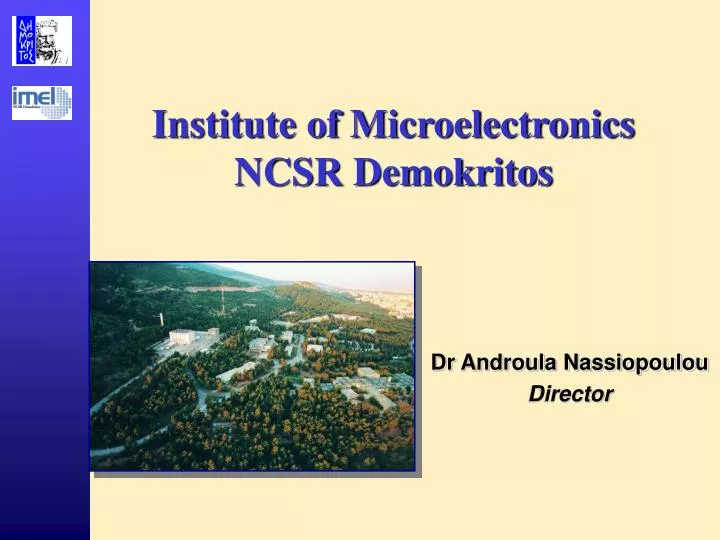
Institute of Microelectronics NCSR Demokritos Dr Androula Nassiopoulou Director
Ministry of Development ORGANIZATIONAL STRUCTURE OFNCSR DEMOKRITOS General Secretariat for Research and Technology NCSR DEMOKRITOS Central administration Department for Technical Support Secretariat of Special Accounts Liaison Office Technology Park Institute of Microelectronics (IMEL) Institute of Nuclear Physics Institute of Nuclear Technology Institute of MaterialsScience Institute of Chemistry Institute of Informatics and Telecommunications Institute of Biology Institute of Radioisotopes & Radiodiagnostic Products
ACADEMIC AND TECHNOLOGICAL EXCELLENCE AT IMEL IMEL: 20 years of research and technology development Achievements: • Infrastructure and research facilities for Micro andNanotechnology unique in Greece • Fully equipped silicon processing laboratory • E-beam lithography equipment • Micromachining and Sensor laboratory • Fully equipped laboratory for characterization of materials, devices and structures • Important know-how • Experienced personnel • An Intellectual property portfolio, which continues to expand
IMEL Institute Director International Scientific Advisory Committee Institute Administration and Technical Support Institute Advisory Board Secretariat Education and training Managerial office - provisions Group of technicians for technical support Program I: Micro and Nanotechnologies Program III: Micro and Nano-Systems Program II: Micro and Nanoelectronics Services in Micro, Nanotechnologies and Microsystems Central facilities for Silicon Processing
PATTERNING TECHNOLOGIES Lithography and Plasma Etching FOCUS OF RESEARCH Development of novel materials, processes and process simulation methods for micro and nanofabrication Key Researchers: M. Hatzakis, IBM fellow and ex-director of IMEL E. Gogolides P. Argitis N. Glezos
Frontiers in Lithography (193 / 157nm, EUV, e-beam), Nano-patterning, MEMS and BioMEMS patterning • Smaller Devices Smaller λ in optical lithography:193, 157nm, EUV, e-beam • Bio Mems Patterning • Need to develop new resists and processes • Thick (0.4μm) to Ultra thin (0.15μm) resist films • Need to increase plasma resistance of photoresists • Critical dimension becomes less than 70nm • Need to Reduce Line Edge Roughness The problems • Develop new resists: aliphatic to fluorinated or Silicon containing polymers • Develop new environmentally friendly and biocompatible photoresists • Add etch resistance compounds in resist formulation • Understand and Simulate Line Edge Roughness using Fractal Theory • Develop lithography and plasma etching simulators • Develop new etching processes for MEMS and Nanotechnology The solutions
Frontiers in Optical Lithography (193 - 157 nm) New resists for 193nm lithography Single layer acrylate. Positive, 93nm lines, Negative 150nm lines; P. Argitis et al. Greek Patent C. Diakouakos et al. Microelec. Engng. 2001 Bilayer resist for 157nm based on Siloxanes. 70nm lines A. Tserepi et al., J. Vac. Sci. Technol. Nov. 2000, Microelec. Engng. 2001 Novel etch resistance compounds synthesized for use as resist additives
Si and SiO2 Etching in Fluorocarbon Plasmas Dielectric Etching, Optoelectronics and MEMS etching • Fluorocarbon plasma and HDP reactors used • Both Experimental and Theoretical Work • Many problems (RIE lag, etch stop, Inverse RIE lag, roughness) • New processes needed in ICP tools, with reduced roughness, for both MEMS and Nanotechnology • Detailed models for etching in fluorocarbon plasmas • Prediction of ASPECT RATIO dependent phenomena
SEMICONDUCTOR NANOSTRUCTURES. Materials, Processes, Properties and Nanoelectronic Devices FOCUS OF RESEARCH • Nanopatterning (nanostructuring using the “top-down” approach) • Silicon nanocrystal growth and characterization • Si/SiO2 multilayers and superlattices • Si/CaF2 multilayers and superlattices • Silicon and Germanium nanocrystals in SiO2 by different techniques • Nanoelectronic devices for memory, light emitting and other applications • Theoretical work, process and device modeling Key Researchers: A.G. Nassiopoulou D. Tsoukalas P. Normand
Si-Nanocrystal MOS Memory Devices Obtained by Low-Energy Ion-Beam-Synthesis Candidates for Non-Volatile Dynamic Memory Applications ESSDERC’2000, Appl. Phys. Lett. 2000
SILICON SENSORS AND MICROSYSTEMS FOCUS OF RESEARCH • Silicon micromachining techniques and processes • Silicon sensor devices and microsystems • Modeling, characterization and testing of sensors • Microsystem design, fabrication and characterization • Development of read-out electronics and packaging
100μm NOVEL PROCESS FOR THE FABRICATION OF SUSPENDED MEMBRANES FOR THERMAL SENSORS • The process is based on the isotropic etching of silicon using High Density Plasma etching. • High lateral etch rates can be achieved (6-7μm/min). • The process is CMOS compatible. • Oxide/nitride membranes with dimensions 100x100μm2, can be easily fabricated.
Apply wafer bonding technique WAFER BONDING USED IN SENSOR TECHNOLOGY Pressure sensors Dry release processes and vapour sensing A technology to combine heterogeneous functions
3D View of pressure Sensor SEM cross section images
COMBINING DRY RELEASED CANTILEVERS WITH POLYMERS TO MEASURE HUMIDITY Parallel beam to substrate Stress effect
INTEGRATED SILICON OPTICAL BIOSENSORS • Monolithically Integrated Silicon Light Emitters, Optical Fibers and Detectors. • Optical Coupling Efficiency 40%. • High Stable and Repeatable Measurements of the Detector Photocurrent. • Five Mask Process with Standard IC Technology
MICROELECTRONIC DESIGN FOR FUTURE OE LINKS FOCUS OF RESEARCH • Develop innovative ICs for optoelectronic links • Implement phenomenological models for optoelectronic devices (photodiodes, VCSELs, etc.) in IC design environment • Develop a wafer-scale integration technology for high-density OE links
IMEL’s infrastructure 1 • Silicon processing equipment (unique in Greece) • Clean room area of 300 m2 • Laminal flow chemical benches • Thermal processing • Chemical Vapor Deposition • Thermal evaporation (sputtering, e- gun evaporation) • Ion implantation • Optical lithography systems • Electron beam lithography system • Plasma Processing (RIE, ICP) • Process Inspection equipment
IMEL’s infrastructure 2 • Characterization equipment • Electrical characterization equipment • Probe stations • Optical characterization • Microscopy equipment, ellipsometry • Sensor characterization (gas, flow, pressure) • Packaging equipment (Dicing saw, wire bonding, die bonder) • Chemistry laboratory • Design and modeling / simulation tools • 7 Workstations (2HP C160, 1HP 9000/785, 2 Sun Sparc 20, 2 Sun Sparc Ultra 1, 1HP 9000/720) • Design software (Mentor graphics: 4 seats, Cadence: 2 seats, synopsis: 2 seats, orcad for PCBs), MEMCAD 4.6, ANSYS and Silvaco softwares.
EDUCATION AND TRAINING DEVELOPMENT OF HUMAN RESOURCES IMEL COORDINATES AN EDUCATIONAL PROGRAMME (EPEAEK) ON MICROELECTRONICS FOR MASTER AND PhD DEGREES-IN COLLABORATION WITH THE UNIVERSITY OF ATHENS Start-date :1/10/1998 Duration of the programme related to the MSc degree : 18 months Duration of PhD cycle : 4 years Number of students : 15 / year • IMEL is partly engaged in two other MSc and PhD programs in collaboration with the National Technical University of Athens (New materials) and the University of Patras (System design) respectively. • IMEL organizes every year : • Summer Schools on selected areas, addressed to graduate students. • Training courses, addressed to research scientists, engineers and technicians. • Conferences, workshops etc.
YEAR 2002 A CENTER OF EXCELLENCE IN MICRO, NANOTECHNOLOGIES AND MICROSYSTEMS AT IMEL/NCSR “DEMOKRITOS” A Center of Excellence in Micro, Nanotechnologies and Microsystems has been established in the year 2002 at IMEL/NCSR “Demokritos”, supported by the Greek General Secretariat for Research and Technology in the Ministry of Development.
MAIN OBJECTIVES • To further promote long term research into understanding phenomena, mastering processes and developing research tools. • To promote development of fundamental knowledge • To promote development of novel products and production processes • To develop human potential by educational and training activities • To develop the access to services in advanced processes and high technology • To promote the transfer of technology to industry. • To further promote cooperative research and technological and educational activities
RESEARCH ACTIVITIES IN THE ABOVE FIELDS • Micro and Nanofabrication • Optical lithography and lithographic materials • Electron beam lithography. • Etching processes • Thermal processes • Thin film deposition techniques • Nanoelectronic devices for integrated circuits • Single electron transistors, resonant tunneling devices, molecular devices and interconnections of devices • Optical and optoelectronic links • Self-assembled building blocks for nanoscale ICs • New electronic materials • Seniconductor nanocrystals and other low dimensional structures in different isolating matrices • Molecular materials • Microsystems and Sensors
MMN Greek Network on Microelectronics, Microsystems and Nanotechnology Main objectives • To promote collaboration between all national organizations involved in Microelectronics, including research centers, universities and private sector. • To develop mechanisms to promote awareness of worldwide scientific and technological development • To develop cooperative educational and training activities, in order to increase the human potential of trained people in the above technologies