Download
1 / 15
150 likes | 293 Vues
2009 ITRS Emerging Research Materials [ERM] July 15, 2009. Michael Garner – Intel Daniel Herr – SRC. James Jewett Intel Ted Kamins HP Sean King Intel Atsuhiro Kinoshita Toshiba Yi-Sha Ku ITRI Wei-Chung Lo ITRI Louis Lome IDA Cons. Allan MacDonald Texas A&M

E N D
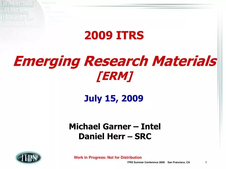
2009 ITRSEmerging Research Materials[ERM]July 15, 2009 Michael Garner – Intel Daniel Herr –SRC
James Jewett Intel Ted Kamins HP Sean King Intel Atsuhiro Kinoshita Toshiba Yi-Sha Ku ITRI Wei-Chung Lo ITRI Louis Lome IDA Cons. Allan MacDonald Texas A&M Francois Martin LETI Fumihiro Matsukura Tohoku U. Yoshiyuki Miyamoto NEC Paul Nealey U. Wisc. Fumiyuki Nihey NEC Dmitri Nikonov Intel Yaw Obeng NIST Chris Ober Cornell Univ. Jeff Peterson Intel Ramamoorthy Ramesh U.C. Berkeley Paolo Rapposelli Intel Nachiket Raravikar Intel Curt Richter NIST Dave Roberts Nantero Jae Sung Roh Hynix Tadashi Sakai Toshiba Mitusru Sato TOK Sadasivan Shankar Intel Shintaro Sato Fujitsu Hideyuki Sasaki NanoAnalysis Corp Atsushi Shiota JSRMicro Kaushal Singh AMAT Tsung-Tsan Su ITRI Naoyuki Sugiyama Toray Raja Swaminathan Intel Takashi Kariya Ibiden Yoshihiro Todokoro NAIST Yasuhide Tomioka AIST Peter Trefonas Rohm Haas Toyohiro Chikyow NIMS Ming-Jinn Tsai ITRI Ken Uchida TI Tech Yasuo Wada Toyo U Vijay Wakharkar Intel Kang Wang UCLA Rainer Waser Aacken Univ. Jeff Welser IBM/NRI C.P. Wong GA Tech. Univ. H.S. Philip Wong Stanford University Hiroshi Yamaguchi NTT Toru Yamaguchi NTT Chin-Tien Yang ITRI Yuegang Zhang LBNL Victor Zhirnov SRC Chuck Zmanda Rohm Haas HiroAkinaga AIST Nobuo Aoi Matsushita Koyu Asai Renesas Yuji Awano Fujitsu Rama Ayothi JSR Daniel-Camille Bensahel STM Bill Bottoms Nanonexus George Bourianoff Intel Alex Bratkovski HP Bernard Capraro Intel John Carruthers Port. State Univ. An Chen AMD Zhihong Chen IBM Byung Jin Cho KAIST U-In Chung Samsung Luigi Colombo TI Hongjie Dai Stanford Univ. Jean Dijon LETI Catherine Dubourdieu L. Mat. Genie Phys. Satoshi Fujimura TOK Michael Garner Intel Emmanuel Giannelis Cornell Univ. Michael Goldstein Intel Dan Herr SRC Bill Hinsberg IBM Jim Hutchby SRC Saori Ishizu AIST Kohei Ito Keio Univ. Ajey Jacob Intel 2008 - 2009 ERM Participants
2009 Key Messages • 2009 ERM Chapter will focus applications • Materials for ERD Devices • Lithography • Front End Processes • Interconnects • Assembly and Package • Establish Critical Assessment Process • Alternate Channel Materials, etc.
Extending CMOS Alternate Channel Materials MOS Alternate Channel Materials -Ge & III-V Compounds -Nanowires -Graphene -Carbon Nanotubes Assess Materials Performance Gate materials Contacts Interfaces III-V Heterostructures (L. Samuelson, Lund Univ.) A. Geim, Manchester U. -Also Identify Novel Metrology & Modeling Needs D. Zhou, USC
Beyond CMOS Materials & Interfaces States Other Than Charge Only Charge Based Ferroelectric Polarization Spin State Assess • Ferromagnetic Materials, Dilute Magnetic Semiconductors • Complex Metal Oxides • Strongly Correlated Electron State Materials (FE, FM, FE & FM) • Molecules • Interfaces • Individual or • Collective Negative Capacitance FET
Memory Complex Metal Oxides & Transition Metal Oxides • Capacitive • FeFET • Resistive Memory • Nanoelectromechanical • STT • Nanothermal • Nano-ionic • Electronic Effects • Molecular Ferromagnetic Materials Chalcogenides Nanotubes & Nanowires Macromolecules
Dendrimers, Frechet, UC-B Lithography Novel Molecules for Double Exposure Evolutionary Resist Design -Positive Resist Tethered Anthracene New Applications of Old Resist Non-Chem Amp (193nm) Negative Resist (EUV) Intermediate State Bristol, Intel Directed Self Assembly Novel Molecules Resist Molecular Glasses Ober, Cornell Hinsberg, IBM
Monolayer Doping Javey, UCB Front End Processing & PIDS Materials Deterministic Doping STM Dopant Placement • Directed Self Assembly for • Selective etch • Selective deposition • Selective protection in clean operations Simmons, U. New S. Wales • Proposals for Massive parallel precision implants Vt set by the number of dopant atoms in the channel depletion region
Wire Wire Via Via Interconnect Materials Interconnects • Ultra-thin Barrier Layers • Transition Nitride (ZrN, HfN, ZrGeN,...) • Direct Plate (Ir, Os, Rh, ...) • SAM Ultra low κ ILD Novel Interconnects & Vias - Carbon Nanotubes Y. Awano,Fujitsu -Graphene -Single Crystal Metal Nanowires
Emerging Packaging Applications Thermal Nanotubes • Package Thermo-Mechanical • Substrate: Nanoparticles, Macromolecules • Adhesives: Macromolecules, Nanoparticles • Chip Interconnect: Nanoparticles • Polymers: Nanoparticles & Macromolecules • High Density Power Delivery Capacitors • Dielectrics: High K • Self Assembly • Interconnects: Nanotubes or Nanowires
Hexagon of Assembly Material Requirements Examples Thermal Interface Mat. Mold Compound Underfill Adhesives Epoxy Functional Properties • Highly coupled Material Properties • Apply novel materials to achieve optimal performance Moisture Resistance Adhesion Fracture Toughness Modulus CTE
ESH Challenges • Materials needed to overcome significant technical challenges • Few materials could meet requirements • Materials have known or uncharacterized EHS properties • Stimulate ESH research in uncharacterized materials • Encourage development of BKM for materials EHS in Research, Development & HVM • Efficient use of materials • Manufacturing in highly controlled environments
Emerging Metrology and Modeling Needs • Metrology • Chemical and structural imaging and dimensional accuracy at the nm scale • Low dimensional material properties (Mapping) • Nondestructive nanoscale embedded interface characterization • Simultaneous dynamic spin and electrical properties • nm scale characterization of vacancies and defects and effects on electronic properties • Modeling Materials and Interfaces • Low dimensional material synthesis & properties • Spin material properties • Strongly correlated electron material properties • Anion & cation vacancy effect on electronic properties • Integrated models and metrology (de-convolution of nm scale metrology signals) • Metrology and modeling must be able characterize and predict performance and reliability
Summary • ERM identifies and assesses materials as potential solutions for ITWG applications • Significant challenges must be addressed for these materials to be viable for transfer to the ITWGs • Complete 2009 ERM Chapter


![2011 ITRS Emerging Research Materials [ERM] July 10-13, 2011](https://cdn2.slideserve.com/4220097/2011-itrs-emerging-research-materials-erm-july-10-13-2011-dt.jpg)