Content
EELE 2321 – Electronics Spring, 2013 Bipolar Junction Transistor (BJT) Structure Eng. Wazen M. Shbair. Content. Bipolar Junction Transistor (BJT) BJT parameters and characteristics Collector Characteristic Curves. The BJT as Amplifier. Bipolar Junction Transistor.

Content
E N D
Presentation Transcript
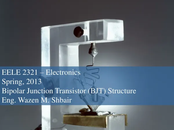
EELE 2321 – Electronics Spring, 2013 Bipolar Junction Transistor (BJT) StructureEng. Wazen M. Shbair
Content • Bipolar Junction Transistor (BJT) • BJT parameters and characteristics • Collector Characteristic Curves. • The BJT as Amplifier.
Bipolar Junction Transistor • The BJT is constructed with three doped semiconductor regions separated by two pn junctions • Three regions are called emitter, base, and collector.
BJT Operation • BJT to operate properly as an amplifier, the two pn junctions must be correctly biased with external dc voltages.
Transistor Currents • The directions of the currents in an npn transistor and its schematic symbol. • These diagrams show that the emitter current (IE) is the sum of the collector current (IC) and the base current (IB)
BJT parameters and characteristics • The dc current gain of a transistor is the ratio of the dc collector current (IC) to the dc base current (IB) and is designated dc βDC. • The ratio of the dc collector current (IC) to the dc emitter current (IE) is the dc alpha αDC
Example VBE= 0.7 v IB=430 MA IC=64.5 mA IE=64.9 VCE=3.55v VCB=2.85 v
Collector Characteristic Curves BJT Characteristics The collector characteristic curves show the relationship of the three transistor currents. The curve shown is for a fixed based current. The first region is the saturation region. Breakdown region Active region As VCE is increased, IC increases until B. Then it flattens in region between points B and C, which is the active region. Saturation region After C, is the breakdown region.
Collector Characteristic Curves BJT Characteristics The collector characteristic curves illustrate the relationship of the three transistor currents. By setting up other values of base current, a family of collector curves is developed. bDCis the ratio of collector current to base current. It can be read from the curves. The value of bDC is nearly the same wherever it is read.
Collector Characteristic Curves BJT Characteristics Example: What is the bDC for the transistor shown? Solution: Choose a base current near the center of the range – in this case IB3 which is 30 mA. Read the corresponding collector current – in this case, 5.0 mA. Calculate the ratio: 167
Collector Characteristic Curves Cutoff In a BJT, cutoff is the condition in which there is no base current, which results in only an extremely small leakage current (ICEO) in the collector circuit. For practical work, this current is assumed to be zero. In cutoff, neither the base-emitter junction, nor the base-collector junction are forward-biased.
Collector Characteristic Curves Saturation In a BJT, saturation is the condition in which there is maximum collector current. The saturation current is determined by the external circuit (VCC and RC in this case) because the collector-emitter voltage is minimum (≈ 0.2 V) In saturation, an increase of base current has no effect on the collector circuit and the relation IC = bDCIB is no longer valid.
Collector Characteristic Curves DC Load Line Example: What is the saturation current and the cutoff voltage for the circuit? Assume VCE = 0.2 V in saturation. Solution: 4.48 mA 15 V Follow-up: Is the transistor saturated? IC = bIB = 200 (10.45 mA) = 2.09 mA Since IC < ISAT, it is not saturated.
BJT as a voltage amplifier • Amplification is the process of linearly increasing the amplitude of an electrical signal. • a BJT exhibits current gain (called b). When a BJT is biased in the active (or linear) region, the BE junction has a low resistance due to forward bias and the BC junction has a high resistance due to reverse bias.
BJT as a voltage amplifier DC and AC Quantities The text uses capital letters for both AC and DC currents and voltages with rms values assumed unless stated otherwise. DC Quantities use upper case roman subscripts. Example: VCE. (The second letter in the subscript indicates the reference point.) AC Quantities and time varying signals use lower case italic subscripts. Example: Vce. Internal transistor resistances are indicated as lower case quantities with a prime and an appropriate subscript. Example: re’. External resistances are indicated as capital R with either a capital or lower case subscript depending on if it is a DC or ac resistance. Examples: RC and Rc.
Voltage Amplification • A transistor amplifies current because the collector current is equal to the base current multiplied by the current gain, β. • The base current in a transistor is very small compared to the collector and emitter currents. • The collector current is approximately equal to the emitter current.
Voltage Amplification A BJT amplifies AC signals by converting some of the DC power from the power supplies to AC signal power. An ac signal at the input is superimposed in the dc bias by the capacitive coupling. The output ac signal is inverted and rides on a dc level of VCE.
BJT Switch A BJT can be used as a switching device in logic circuits to turn on or off current to a load. As a switch, the transistor is normally in either cutoff (load is OFF) or saturation (load is ON). In cutoff, the transistor looks like an open switch. In saturation, the transistor looks like a closed switch.
End Of Chapter 4. • Home work for Charter 3&4 will be announced on MOODEL. • Next Monday(4/3/2013)we will have Quiz on Chapter 4.


