Download
1 / 35
350 likes | 452 Vues
This document provides a detailed analysis of the TMS320C6000 architecture, focusing on the register operations and supporting data paths that enhance processing power. It discusses the 32-bit and 40-bit registers, their configurations, and how operands can be manipulated within the architecture. The text highlights the importance of register-to-register data transfer, increasing processing capabilities, and the implementation of cross paths for data exchange between processing units. This information is critical for understanding design and operational enhancements in the TMS320C6000 chip.

E N D
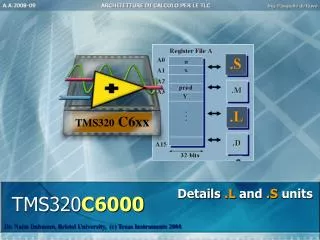
TMS320 C6xx TMS320C6000 Details .L and .S units Dr. Naim Dahnoun, Bristol University, (c) Texas Instruments 2004
Register File A .S A0 A1 A2 A3 A15 a x .M prod Y .L ... .D .D 32-bits Data Memory Details .L and .S units OPERAZIONI ARITMETICO LOGICHE General Purpose OPERANDI CO.U <? >, <?> , <?>
OPERANDS32/40-bits Register, 5-bits Constant • OPERANDS can be: • 5-bit constants(or 16bitfor MVKL and MVKH) • 32-bit registers • 40-bit Registers However, we have seen that registers are only 32-bit. So where do the 40-bit registers come from?
OPERANDS40-bits Register A 40-bit register can be obtained by concatenating two registers There are 3 conditions that need to be respected: • The registers must be from the same side. • The first register must be even and the second odd. The registers must be consecutive.
40-bit Reg 40-bit Reg : : even even odd odd 8 8 32 32 A1:A0 A3:A2 A5:A4 A7:A6 A9:A8 A11:A10 A13:A12 A15:A14 B1:B0 B3:B2 B5:B4 B7:B6 B9:B8 B11:B10 B13:B12 B15:B14 OPERANDS40-bits Register All combinations of 40-bit registers are shown below:
32-bitReg 40-bitReg 5-bitConst 32-bitReg < src > < src > .L or .S < dst > 32-bitReg 40-bitReg OPERANDS32/40-bits Register, 5-bits Constant instr .unit <SRC>, <SRC>, <DST>
32-bitReg 40-bitReg 5-bitConst 32-bitReg < src > < src > < dst > 32-bitReg 40-bitReg Operands32/40-bits Register, 5-bits Constant instr .L <SRC>, <SRC>, <DST> .L or .S
32-bitReg 40-bitReg 5-bitConst 32-bitReg < src > < src > < dst > 32-bitReg 40-bitReg Operands32/40-bits Register, 5-bits Constant instr .L <SRC>, <SRC>, <DST> .L or .S OR .L1 A0, A1, A2
32-bitReg 40-bitReg 5-bitConst 32-bitReg < src > < src > < dst > 32-bitReg 40-bitReg Operands32/40-bits Register, 5-bits Constant instr .L <SRC>, <SRC>, <DST> .L or .S OR .L1 A0, A1, A2 ADD .L2 -5, B3, B4
32-bitReg 40-bitReg 5-bitConst 32-bitReg < src > < src > < dst > 32-bitReg 40-bitReg Operands32/40-bits Register, 5-bits Constant instr .L <SRC>, <SRC>, <DST> .L or .S OR .L1 A0, A1, A2 ADD .L2 -5, B3, B4 ADD .L1 A2, A3, A5:A4
32-bitReg 40-bitReg 5-bitConst 32-bitReg < src > < src > < dst > 32-bitReg 40-bitReg Operands32/40-bits Register, 5-bits Constant instr .L <SRC>, <SRC>, <DST> .L or .S OR.L1 A0, A1, A2 ADD.L2 -5, B3, B4 ADD.L1 A2, A3, A5:A4 SUB.L1 A2, A5:A4, A5:A4
32-bitReg 40-bitReg 5-bitConst 32-bitReg < src > < src > < dst > 32-bitReg 40-bitReg Operands32/40-bits Register, 5-bits Constant instr .L <SRC>, <SRC>, <DST> .L or .S OR.L1 A0, A1, A2 ADD.L2 -5, B3, B4 ADD.L1 A2, A3, A5:A4 SUB.L1 A2, A5:A4, A5:A4 ADD.L2 3, B9:B8, B9:B8
TMS320 C6xx Register to RegisterData Transfer TMS320C6000 Dr. Naim Dahnoun, Bristol University, (c) Texas Instruments 2004
Register to Register Data Transfer To move the content of a Register (A or B) to another register (B or A) use the move MV Instruction, e.g.: MV A0 , B0 or MV B6 , B7 To move the content of a Control Register to another register (A or B) or vice-versa use the MVCinstruction, e.g.: MVC IFR , A0 or MVC A0 , IRP
TMS320 C6xx TMS320C6000 Increasing the processing power Dr. Naim Dahnoun, Bristol University, (c) Texas Instruments 2004
Register File A .S A0 A1 A2 A3 A15 .M .L ... .D .D 32-bits Data Memory How can we add more processing power to this processor? Increasing the processing power!
Register File A .S A0 A1 A2 A3 A15 .M .L ... .D .D 32-bits Data Memory Increase the clock frequency Increasing the processing power! Increase the number of Processing units
Scambio di operandi RegisterFile A Register File B .S1 .S2 A0 B0 A1 B1 A2 B2 .M1 .M2 A3 B3 A4 B4 .L1 .L2 ... ... .D1 .D2 A15 B15 Scambio di operandi 32-bits 32-bits Data Memory To increase the Processing Power, this processor has Two Sides Increasing the processing power!
Increasing the processing power! To exchange operands between the two sides, some CROSS PATH or LINKS are required What is a CROSS PATH? • A Cross Path links one side of the CPU to the other • There are two types of Cross Paths: • DATACROSS PATH • ADDRESSCROSS PATH
Data Cross Paths TMS320C6000 Increasing the processing power Dr. Naim Dahnoun, Bristol University, (c) Texas Instruments 2004
Data Cross Paths • Data C.P. = register file C.P. • These cross paths allow operands from one side to be used by the units of the other side • There are only two cross paths: • one path which conveys data from side B to side A, 1X • one path which conveys data from side A to side B, 2X
TMS320 C67x TMS320C67x Data-Path - Summary src = source dst = destination • DATA cross paths only apply to the .L, .S and .M units • The data cross paths are very useful, however there are some limitations in their use.
A .L1 .M1 .S1 <src> <dst> <src> 2x B 1x Data Cross Path - Limitations (1) The Destination register must be on same side as unit (2) Source registers - up to ONE Cross Data Path per execute packet per Side. Execute packet: group of instructions that execute simultaneously.
A .L1 .M1 .S1 <src> <dst> <src> 2x B 1x Data Cross Path - Limitations • ADD .L2x A0 , A1 , B2 • MPY .M1x A0 , B6 , A9 • SUB .S1x A8 , B2 , A8 • ||ADD .L1x A0 , B0 , A2 • || Means that the SUB and ADD belong to the same fetch packet, therefore execute simultaneously. Not Valid ! Source registers - up to ONE Cross Data Path per execute packet per Side
A .L1 .M1 .S1 <src> <dst> <src> 2x 1x B .L2 .M2 .S2 <src> <dst> <src> Data Cross Path - Limitations Valid ! SUB .S1x A8 , B2 , A8 ||ADD .L2x A0 , A0 , B5
ADDRESS Cross Paths TMS320C6000 Increasing the processing power Dr. Naim Dahnoun, Bristol University, (c) Texas Instruments 2004
A Data .D1 Addr Address paths LDW .D1T1*A0, A5 STW .D1T1A5, *A0 The pointer must be on the same side of the unit
Address Cross Paths A Data1 A5 DA1 = T1 .D1 *A0 LDW .D1T1 *A0,A5 LDW .D1T2 *A0,B5 B DA2 = T2 .D2 Data2 B5
Standard Parallel Loads Data1 A5 A .D1 DA1 = T1 *A0 B .D2 DA2 = T2 *B0 LDW .D1T1 *A0,A5 || LDW .D2T2 *B0,B5 B5
Parallel Load/Store using Address Cross Paths A Data1 A5 .D1 DA1 = T1 *A0 B .D2 DA2 = T2 *B0 LDW .D1T2 *A0,B5 || STW .D2T1A5,*B0 B5
Fill the blanks ... Does this work? A Data1 .D1 DA1 = T1 *A0 .D2 B DA2 = T2 *B0 LDW .D1__ *A0,B5 || STW .D2__ B6,*B0
Not Allowed! Parallel accesses: both cross or neither cross A Data1 .D1 *A0 .D2 B DA2 = T2 *B0 B5 B6 LDW .D1T2 *A0,B5 || STW .D2T2B6,*B0
TMS320 C67x CPU Ref Guide Full CPU Datapath(Pg 2-2) ‘C67x Address Data-Path - Summary
Conditions Don’t Use Cross Paths Examples:[B2] ADD .L1 A2,A0,A4 // [A1] LDW .D2 *B0,B5 If aconditional registercomes from the opposite side, it does NOT use a data or address cross-path.
Cross Paths - Summary • Data • Destination register on same side as unit. • Source registers - up to one cross path per execute packet per side. • Use “x” to indicate cross-path. • Address • Pointer must be on same side as unit. • Data can be transferred to/from either side. • Parallel accesses: both cross or neither cross. • ConditionalsDon’t Use Cross Paths.