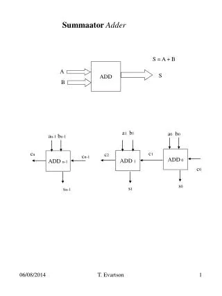
Half Adder
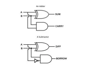
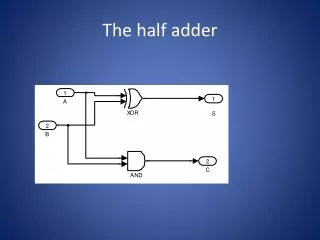
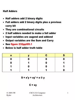
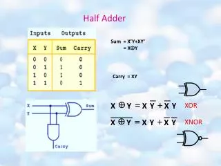
Å. =. +. X. Y. X. Y. X. Y. Half Adder. Sum = X’Y+XY’ = X Y. Carry = XY. XOR. XNOR. Å. =. +. X. Y. X. Y. X. Y. Full Adder. SUM=. Carry Out=. Sequential Logic Circuits. Comparison Between CLC & SLC. CLC. Output. Input.

Half Adder
E N D
Presentation Transcript
Å = + X Y X Y X Y Half Adder Sum = X’Y+XY’ = XY Carry = XY XOR XNOR Å = + X Y X Y X Y
Full Adder SUM= Carry Out=
Sequential Logic Circuits Comparison Between CLC & SLC CLC Output Input Unlike Combinational logic circuits that change state depending upon the actual signals being applied to their inputs at that time, Sequential Logic circuits have some form of inherent "Memory" built in to them and they are able to take into account their previous input state as well as those actually present a sort of "before" and "after" is involved.
They are generally termed as Two State or Bistable devices which can have their output set in either of two basic states, a logic level "1" or a logic level "0" and will remain "Latched" indefinitely in this current state or condition until some other input signal or data is applied which will changes its state once again. The word "Sequential" means that things happen in a "sequence", one after another and in Sequential Logic circuits, the actual clock signal determines when things will happen next. Sequential Logic circuits can be divided into 3 main categories: 1. Clock Driven - Synchronous Circuits that are Synchronized to a specific clock signal. 2. Event Driven - Asynchronous Circuits that react or change state when an external event occurs. 3. Pulse Driven - Which is a Combination of Synchronous and Asynchronous.
Flip Flops (Bistable Multivibrator) Simple sequential logic circuits can be constructed from standard Bistable circuits such as Flip-flops. The term "Flip-flop" relates to the actual operation of the device, as it can be "Flipped" into one logic state or "Flopped" back into another. • RS Latch • Reset-Set (RS) Flip Flop • J-K Flip Flop • Toggle (T) Flip Flop • Data Storage (D) Flip Flop
The SR Latch An SR Flip-Flop can be considered as a basic one-bit memory device that has two inputs, one which will "SET" the device and another which will "RESET" the device back to its original state and an output Q that will be either at a logic level "1" or logic "0" depending upon this Set/Reset condition. S R Q Q’ S R Q Q’
Clocked SR Flip-Flop S CLK R N1 Q Q’ N3 Q Q’ S CLK R N4 N2
The JK Flip-flop N1 J CLK K Q Q’ N3 Q Q’ J CLK K N4 N2
The D & T Flip-flops T D J CLK K Q Q’ J CLK K Q Q’
Counters • Synchronous counters • Asynchronous counters Synchronous Pertaining to two or more processes that depend upon the occurrence of specific events such as common timing signals. counter A functional unit with a finite number of states each of which represents a number that can be, upon receipt of an appropriate signal, increased by unity or by a given constant. So a "synchronous counter" is actually a functional unit with a certain number of states, each representing a number which can be increased or decreased upon receiving an appropriate signal (e.g. a rising edge pulse), and is usually used to count to, or count down to zero from, a specified number N.
Shift Register Shift Registers are mainly used to store data and to convert data from either a serial to parallel or parallel to serial format with all the latches being driven by a common clock (Clk). Shift Registers consists of a number of single bit "D-Type Data Latches" connected together in a chain arrangement so that the output from one data latch becomes the input of the next latch and so on, thereby moving the stored data serially from either the left or the right direction. Generally, Shift Registers operate in one of four different modes: Serial-in to Parallel-out (SIPO) Serial-in to Serial-out (SISO) Parallel-in to Parallel-out (PIPO) Parallel-in to Serial-out (PISO)
Serial-in to Serial-out Parallel-in to Serial-out