Download
1 / 53
530 likes | 806 Vues
Near and Far-infrared Photon. Detection Techniques. in Semiconductors. Viraj Jayaweera Department of Physics Astronomy. Outline. Introduction Dye-Sensitized Near-Infrared Detectors (DSID) 1/f Noise in DSID Split-off Band Near-Infrared Detectors

E N D
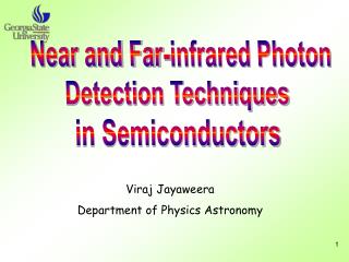
Near and Far-infrared Photon Detection Techniques in Semiconductors Viraj Jayaweera Department of Physics Astronomy
Outline • Introduction • Dye-Sensitized Near-Infrared Detectors (DSID) • 1/f Noise in DSID • Split-off Band Near-Infrared Detectors • Interfacial Workfunction Internal Photoemission (IWIP) Far-Infrared Detectors • Future Studies
The Electromagnetic Spectrum http://www.nasa.gov/centers/langley/science near-IR mid-IR Far-IR Visible Micro wave 0.8 – 5 m 5 - 30 m 30 - 300 m Wavelength
1-3 μm Short Wavelength Infrared SWIR 3-5 μm Medium Wavelength Infrared MWIR 5-14 μm Long Wavelength Infrared LWIR 14-30 μm Very Long Wavelength Infrared VLWIR 30-100 μm Far Infrared FIR 100-1000 μm Submillimeter SubMM IR Wavelength Range Classification
Applications Human Suspect climbing over fence at 2:49 AM in total darkness Infrared image of Orion
Applications Breast Cancer Blood Flow
Applications Loose contacts Bad Insulation spots Electrical Hotspots Energy Conservation
Different Types of Infrared Detectors IR Detectors Photon Detectors Thermal Detectors Pyroelectric Detectors Photo Conductive Photovoltaic Bolometer Thermopile
Dye-Sensitized Near-Infrared Detectors (DSID) n-TiO2 nanoparticle p-CuSCN Dye Dye p-type n-type V http://shs.starkville.k12.ms.us/~kb1/Hort1wk4.htm
Direct and Sensitized Photo-Injection CB CB VB VB Semiconductor Dye Light induced charge carrier generation in a semiconductor Dye-sensitized electron injection to a semiconductor
CTO Transparent CTO Glass n-TiO2 Dye Glass p-CuSCN Platinum or Gold layer Structure of Dye-Sensitized IR Detector TiO2nanoparticles
Energy Level Diagram Appl. Phys. Lett., Vol. 85, No. 23, (2004)
IR Absorbing Dyes The number indicates the peak absorption wavelength in nanometers
Spectral Responsivity Appl. Phys. Lett., Vol. 85, No. 23, (2004)
1/f-like Noise Characteristics Spectral power density of noise Where f is frequency, 0<α<2 α = 0 white noise α = 1 pink noise (strict 1 / f) α = 2 brown noise α = 1 α = 0
Sample Preparation for Noise Measurements Conducting Tin Oxide TiO2 R = 56 k Glass Substrate 18 V
Sample Temp. Sensor N2, H2O(g) Heater Vacuum Noise Measurement Setup PC FT Signal Analyzer (SR785) R Low Noise Pre- Amplifier (SR560)
Noise in TiO2 Nanocrystalline Films Adsorbed molecular species such as H2O and I2 can generate 1/f noise These molecular species can produce electron acceptor state on the TiO2 surface. It is suggested that the trapping and detrappng of electrons at the surface states is the cause of noise. TiO2 (N2 ,I2 vapor) α = 1.37 α = 1.25 TiO2 (N2 RH >40%) TiO2 (N2) Semicond. Sci. Technol. 20 (2005) L40-L42 Infrared Phys. Techn. (2006) In Press, Corrected Proof
Noise in TiO2+Dye Nanocrystalline Films The dye coated TiO2 suppresses the 1/f noise Higher relative humidity can partly desorbs dye from TiO2 surface allowing water adsorption. TiO2/N3(N2, RH=70%) TiO2 (N2 ,I2) TiO2 (N2 RH=70%) TiO2/BPR (N2, RH=70%)) TiO2/N3 (N2, RH <40%) TiO2/BPR (N2, RH <40%) Semicond. Sci. Technol. 20 (2005) L40-L42
Dye-Sensitized IR Detector Noise n-TiO2/MC-IR792/p-CuSCN Power spectral density of the dark current noise of the hetrojunction n-TiO2/MC-IR792/p-CuSCN
HIWIP(Homojunction Interfacial Workfunction Internal Photoemission Detectors) Emitter p+ GaAs Barrier Undoped GaAs p+ GaAs Undoped GaAs hν Δ Δ h+ biased zero bias Barrier formed by Homojunction (p-type) Δ comes from doping Absorption is due to free carriers APL 78, 2241 (2001) APL 82, 139 (2003)
HEIWIP(HEterojunction Interfacial Workfunction Internal Photoemission Detectors) Emitter p+ GaAs Barrier AlxGa1-xAs p+ GaAs AlxGa1-xAs hν Δ Δ h+ biased zero bias Barrier formed by Heterojunction (p-type) Δ comes from Al fraction (x) and doping Absorption is due to free carriers Interface is sharp (no space charge) APL 78, 2241 (2001) APL 82, 139 (2003)
Detector Structure (HE0204) Metal Top Contact ~1000 A Emitter 188 Å p GaAs + + p GaAs n Periods Barrier 1250 Å AlGaAs + p GaAs AlGaAs ++ p GaAs Substrate After processing
Split-off Mechanism E Conduction Band IR Photon excites holes from the light/heavy hole bands to the split-off band (Solid Arrow) Excited holes may escape in split-off band or, May scatter into the light/heavy hole bands and then escape (Dashed Arrow) k Ef ΔL/H Heavy Hole Band Light Hole Band ΔSO Split-off Band
Response Mechanism I E Light/Heavy Hole Band k EF ΔL/H Heavy Hole Band Free Carrier Absorption Light Hole Band escape ΔSO Split-off Band Split-off Band The photoexcitation process consists of the standard free carrier absorption.
Response Mechanism II Light/Heavy Hole Band E k EF ΔL/H Split-off Absorption Heavy Hole Band Light Hole Band scattering ΔSO Split-off Band Split-off Band direct photoabsorption to the split-off band, followed by a scattering to the light/heavy hole band.
Response Mechanism III Light/Heavy Hole Band E k Ef ΔL/H Split-off Absorption Heavy Hole Band Light Hole Band ΔSO Split-off Band Split-off Band escape Single indirect photoabsorption into the split-off band.
Response Mechanism IV Light/Heavy Hole Band E k Ef ΔL/H Split-off Absorption Heavy Hole Band escape Light Hole Band scattering ΔSO Split-off Band Split-off Band indirect photoabsorption, followed by a scattering event to the light or heavy hole band.
Quantum Efficiency of Split-off Detector 0.02 Split-off Response Sample 1332 T = 50K Quantum Efficiency 0.01 Free Carrier Response 0.00 2.5 5.0 7.5 10.0 12.5 15.0 Wavelength (µm)
Split-off Detector Response Threshold for mechanism (III) Threshold for mechanism (II / IV)
i p+ i i p+ i p+ i i h+ h+ h+ Advantages • Increased operating Temperature • Use of the split-off band provides increased absorption at short • wavelengths • Increased escape due to high carrier energies • Increased gain due to impact ionization from high energy carriers Δ Δ Dark Current ~e-Δ/kT ESO ESO ESO Δ Δ Δ
Different material will cover different split-off ranges Antimonides – 1-2 µm Arsinides – 3-5 µm Phosphides – 8-15 µm Nitrides – 40-60 µm
GaSb HIWIP THz Detector Metal contact Top Contact EF 5×1018cm-3 p++ 0.1 μm 2×1018cm-3 p+ emitter 0.05 μm p+ GaSb Δ Undoped-GaSb barrier ΔEV GaSb 2 μm 2×1018cm-3 p+ emitter 0.05 μm p+ GaSb 5×1018cm-3 p++ GaSb Substrate Bottom Contact EF Energy
GaSb HIWIP THz Detector IV APPLIED PHYSICS LETTERS 90, 111109 2007
GaSb HIWIP THz Detector Response Frequency (THz) Frequency (THz) 2 15 10 7 15 4 1.5 (a) T = 4.9 K (b) T = 4.9 K 3.7 V 3.4 V 3.0 V 2.0 V 1.0 V 3.0 V 2.0 V 1.0 V 97 μm
Future Studies • Design optimized split-off band detector operating near room temperature for 3 -5 μm range. • Use different material system to cover different wavelength range • e.g. Nitrides – 40-60 µm • Phosphides – 8-15 µm • InGaSb/GaSb HEIWIP design for THz detection • (a) Design single layer HEIWIP detector as first step • (b) Improve performance using multi layer and resonant cavity structures. • (c) Use surface plasmon to enhance detector performance. • (using metal grid pattern on top detector)
Future Studies In0.02Ga0.98Sb 0.2 μm GaSb 2.1 μm In0.02Ga0.98Sb 0.7 μm GaSb Substrate GaSb 0.2 μm In0.02Ga0.98Sb 2.1 μm GaSb 0.7 μm GaSb Substrate
Acknowledgement • Committee Members • Dr. Unil Perera • Dr. Kirthi Tennakone • Dr. Douglas Gies • Dr. Xiaochun He • Dr. Vadym M. Apelcov • Lab Members • Dr. Steve Matsick • Dr. Mohammad Rinzan • Mr. Aruna Weerasekara • Mr. Gamini Ariyawansa • Mr. Ranga Jayasinghe
Extra stuff Extra stuff
Dye p-type n-type n-type Dye p-type
HIWIP(Homojunction Interfacial Workfunction Internal Photoemission Detector) n+ i GaAs n+ doped GaAs e- hν Δ Δ EF ECn zero bias biased Barrier formed by Homojunction (n-type) (Δ comes from doping) JAP 77, 915 (1995)
Detector Mechanisms E E Conduction Band Conduction Band k k ESO Heavy Hole Band Heavy Hole Band Light Hole Band Light Hole Band Split-off Band Split-off Band Intrinsic (InSb, HgCdTe) Quantum Well
In this Presentation… Wavelength (μm)
Split-off Mechanism IR Photon excites holes from the light/heavy hole bands to the split-off band (Solid Arrow) Excited holes may escape in split-off band or, May scatter into the light/heavy hole bands and then escape (Dashed Arrow) E Conduction Band • Transition is entirely in hole bands • Carrier energies are continuous not quantized • Split-off response is inherently broadband k Ef ΔL/H Heavy Hole Band Light Hole Band ΔSO Split-off Band