Initial Timepix3 Testing Results for CERN and Nikhef Chip Mounting
100 likes | 215 Vues
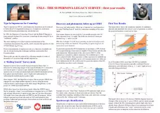
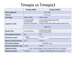
This documentation outlines the first testing results for the Timepix3 sensor chip, mounted at CERN and Nikhef. Initial power-on tests indicated successful operation with no smoke abnormalities. The chip demonstrated a current draw of approximately 780 mA after reset (without clock), and various components were tested. The SLVS interface operated at 40 MHz and the driver successfully managed speeds up to 320 MHz. Key functions, including command decoding and data output at 640 Mbps, were verified. The periphery is about 80% functional, while the pixel matrix remains untested.

Initial Timepix3 Testing Results for CERN and Nikhef Chip Mounting
E N D
Presentation Transcript
Wafer#0 → AAPVX6H @NIKHEF Chip Mounted @CERN W0_J6
Some photos Diced chips in gelpack
First tests • Power ON -> “No Smoke” • ~780mA after Reset (no clock) • Blocks tested: • SLVS IO • receiver at 40MHz (40Mbps) • Driver up to 320MHz (640Mbps) • Command decoder • Receive commands • Sends control commands (END_CMD, ACK_CMD, WRG_CMD and OTHERCHIP_CMD) • Send periphery data output (DAC settings, Timer output…) • PLL • Clearly see in the scope clock multiplication working 40, 80, 160 MHz • Output block • Data received @640Mbps • End Of Column • CTPR load • CTPR read
Data Packet=0x00000 (40-bits) Timer:RequestTimeLow=0x44 END_CMD=0x71 Timer:RequestTimeLow=0x44 ChipID=0x0000
Summary • Start testing on Monday morning • 2 chip mounted: 1 @CERN and 1 @Nikhef • Timepix3 periphery is working as expected • Periphery is ~80% tested • Pixel Matrix not yet tested