Download
1 / 3
30 likes | 178 Vues
Materials Integration of III-V Compounds for Electronic Device Applications . GOALI – DMR -0408715. Mark Goorsky, PI.

E N D
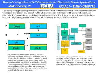
Materials Integration of III-V Compounds for Electronic Device Applications GOALI – DMR -0408715 Mark Goorsky, PI The funding for this project has provided us with the means to understand the basic materials issues associated with wafer bonding and layer transfer. This research enables advancements in the performance of III-V semiconductor devices through the development of wafer bonded template substrates – those with high resistivity and with an appropriate lattice constant for large lattice parameter materials, and with compatible thermal expansion coefficients. Representative schematic of wafer transfer process. a) wafers are coated with silicon nitride; b) transfer wafer is implanted with hydrogen to facilitate exfoliation; c) Nitride surfaces are treated to increase bond strength, bonded at room temperature, and annealed to increase bond strength. The structure can then be heated to higher temperature to cause exfoliation, otherwise, etching and polishing can reduce thickness of the InP (or any layer from a substrate or graded buffer layer to be transferred). Flow chart showing experimental sequences conducted during this research program. The color-coded arrows represent each technology. For example, InAs on InP structures will be subjected to annealing, MBE (InAs and pHEMT) and MOCVD (InAs and InAlAs layer deposition)
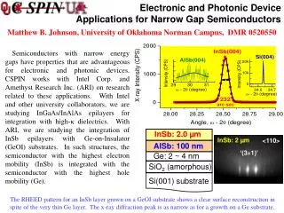
Materials Integration of III-V Compounds for Electronic Device Applications GOALI – DMR -0408715 Mark Goorsky, PI Our publications and continuing research have elucidated key materials issues in the transfer, adhesion mechanisms, chemical-mechanical polishing and thermal stability of III-V semiconductor layers. With this knowledge, we have pioneered the use of layer transfer via hydrogen implantation for a variety of III-V (and IV and II-VI) materials. The broader impact of these advances is now being implemented in on-going SBIR and STTR collaborations. X-ray reflectivity measurements proved an important technique to assess the interfacial bonding mechanisms and high resolution x-ray diffraction represents an ideal means to monitor the exfoliation process in all semiconductor materials. Our transferred InP layers on SiN / GaAs substrates are suitable for MOVPE growth of quantum well (QW) structures as demonstrated with the cross-section TEM image. Our most recent efforts have extended this technology to InAs layer transfer and the transfer of In0.9Al0.1As graded buffer layers to InP substrates. These achievements resulted from a better understanding of how the hydrogen exfoliation process depends on the mechanical and thermal properties of the host material, the hydrogen gettering effect of strained regions and on the diffusivity of hydrogen within the host material. The AFM images on the right show InAs transferred from a bulk substrate and from a graded buffer layer prior to the CMP step. PL (and HRXRD) confirms that the QW structures exhibit comparably strong luminescence and high structural quality as those grown on standard InP substrates and IR transmission measurements confirm that large areas of 3” wafers are successfully bonded.
Materials Integration of III-V Compounds for Electronic Device Applications GOALI – DMR -0408715 Mark Goorsky, PI • Educational and Outreach Activities • In conjunction with the Center for Excellence in Engineering and Diversity at UCLA, we have sponsored undergraduate students to gain research experience in our laboratories. In addition, we have, through CEED, participated in outreach programs through Science and Engineering Days at UCLA. Our demonstrations examining wafer bonding by comparing wafers bonded together in the open air and those bonded within a PMMA “bonding box” provides students with insight into several components of science and engineering: The strength of van der Waals bonds is surprisingly high to the students and discussion of the flatness of the semiconductor wafers helps them appreciate the state-of-the-art in semiconductor processing technology. • Our efforts have continued with the American Indian Science and Engineering Society. In these demonstrations to high school students from throughout the southwest, we demonstrate the issues of thermal expansion coefficients by examining the strength of bonded materials (using adhesives and bonded wafers) at both low (cryogenic) and high temperatures.