Download
1 / 35
360 likes | 654 Vues
Preparation and Characterization of Carbon Nanotubes. Timothy Day and Tyrone Hill ECE 345 November 28, 2001. Overview. Objectives Background Information Original Design Successes and Challenges Testing Conclusions. Project Goals.

E N D
Preparation and Characterization of Carbon Nanotubes Timothy Day and Tyrone Hill ECE 345 November 28, 2001
Overview • Objectives • Background Information • Original Design • Successes and Challenges • Testing • Conclusions
Project Goals • Objective: “To perfect a process for creating H-passivated Si [100] wafers with a sparse enough CNT density to allow manipulation and characterization with an STM.” • 5 nanotubes/square m
Characterization of CNT bonding with Si H-passivated layer Knowledge of CNT electrical properties Recipe for preparing CNT deposition UHV Chamber Atomic Force Microscope Scanning Electron Microscope Scanning Tunneling Microscope Project Features and Equipment
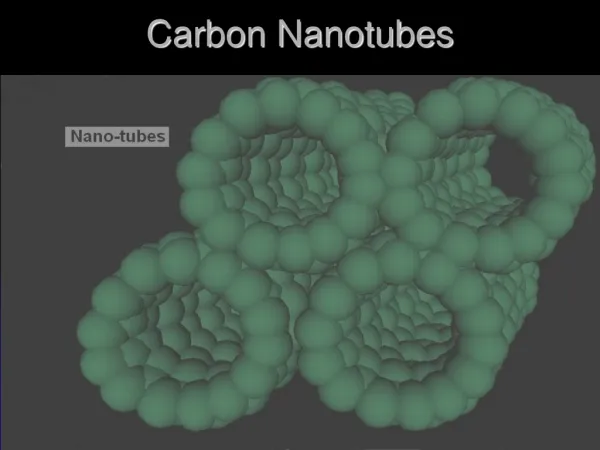
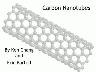
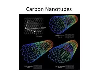
CNT Background Info • Discovered by S. Ijima in 1991 • Tubular hexagonal arrays of graphene sheets • Can be single-walled or multi-walled (~2 nm SWNT diameter) • Have metallic or semiconducting properties • Nanoelectronic Applications
CNT Background Info Chiral vector: • Ch= aV1 + bV2 • Metallic: • a=b • Semi-conducting: • (a-b)=3N • Types: • Armchair: (a,a) • Zigzag : (a,0) • Chiral: (a,b) angle > 30°
Original Design • Degrease Wafers • UHV Passivation • Deposition of CNT • STM/AFM Characterization • Deposit Metal Contacts • Electrical Characterization C60
Ultra High Vacuum System • Main Chamber- Ion Pump w/ base pressure ~5 * 10-11 Torr • Scanning Tunneling Microscope Chamber off main chamber designed by Dr. Lyding • Bake- ~300˚ C for 7 days • Estimated Cost = $300,000
Ultra High Vacuum System DipStick Main Chamber Manipulator STM Load-Lock
Ultra High Vacuum Chamber Basic Operation • Proper Handling of Samples and Sample Holders • Procedure for Inserting Samples into Chamber using load-lock • Maneuvering of Sample Holder with Dipstick and Manipulators
UHV Passivation • Degas Si sample (~700˚ C, 24 hrs) • Cool Dipstick to 40ºC/Perform temperature calibration with pyrometer • Passivation temp: 377° C • Expose Si to two 30 second heat flashes • Introduce H2 gas
UHV Passivation • Step 1: Diatomic Hydrogen (H2) is introduced into the chamber • Step 2: The tungsten “cracking” filament breaks the H bonds • Step 3: The atomic hydrogen atoms attach to the dangling bond on the Si surface
H-Passivation • Dangling Bonds • Dimer rows • Si Terraces • Si Defects
Adjustments and New Directions • Began using “wet” H-passivation • 50:1 HF dip for 30 seconds, DI for 15 seconds, blow dry with N2 gas • Concentrated on CNT deposition • Made 1:10 dilution and 1:100 dilution of original CNT solution • Deposited using volume-controlled syringe • Atomic Force Microscope
Atomic Force Microscope • Two modes: Contact & Tapping* • Tip diameter used was 5-10 nm • Diameter will affect spreading effects • Atomic Resolution • Small Damage Effects • Slow Scanning Speed
Atomic Force Microscopy • 1. Laser • 2. Mirror • 3. Photodetector • 4. Amplifier • 5. Register • 6. Sample • 7. Probe • 8. Cantilever
Environmental Scanning Electron Microscopy • Column generates electron beam that is aimed at sample and focused with EM fields • Images are obtained by detecting and processing primary electron scattering • Resolution of 5-10 nm • Scanning speed faster than AFM
Problems and Solutions • CNTs appeared only in concentrated islands • Amorphous carbon particles contaminated CNT islands • Made new CNT solution • Anthony Bollinger, Physics Dept. UIUC • Dried CNT in DCE • Sonicated for 15 min
Conclusions from ESEM • Use second CNT solution with 1:5 dilution • Sonicate diluted solution for at least 15 min • Deposit 2 L drop and allow solvent(DCE) to evaporate • Scanning Tunneling Microscopy
Scanning Tunneling Microscopy • A biased sharp tip at nm distances causes a tunneling current to flow between sample and tip • Feedback of tunneling current keeps current constant while varying height of tip using a voltage controlled piezoelectric tube • Movements are recorded and converted to topographical map of sample surface
UHV STM Design Piezoelectric Scanning Unit Tunneling Probe Sample Holder
Image After Sample Degas 3000x3000 Å2 -3.5V 4x10-11A Large rope like structure present, as well as, the atomic steps of silicon surface are observed.
Image of Rope Section Initial Image of Bundle Tip is Multiple After Several Scans Bundle Appears to be Unraveling 600x600 Å2 -3.5V 3.25x10⁻¹¹A 600x600 Å2 -3.5V 3.25x10⁻¹¹A
Single Walled Nanotube on Passivated Si(100) 800x800 Å2 -3.5V 4x10-11A ~25Å
Magnified SWNT and DOS Characterization Topography dI/dV 300x300 Å2-3.5V 8.6x10⁻¹²A
Multiple Tip Image of Potential Single Wall Nanotube 650x650 Å2 -3.5V 4x10-12A ~ 17Å Attempted todamage tube using nano- lithography routine, tube was clearly perturbed, but more work is needed before we can draw any conclusions.
Zoom in of Multiple Tip Image of Potential Single Wall Nanotube 450x450 Å2 -3.5V 4x10-12A
Final Conclusions • Possible to image CNTs with STM on semiconducting substrate • Van der Waals interactions make isolation of single tube very difficult • Could get better data with sharper STM tip • Use cleaner solvent to avoid organic contamination
Special Thanks • Dr. Joe Lyding for guidance and use of his facilities • Frankie Liu and Nathan Guisinger for their help and technical expertise • Anthony Bollinger for his CNTs • Matt Olson for his advice