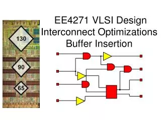
Interconnect Optimizations
Explore interconnect scaling, wire sizing, buffer insertion, and analysis of RC circuits for optimal delay reduction in semiconductor design. Understand the impact of geometries and cross-sections on interconnect performance. Learn about buffer insertion techniques and combinational logic delay. A detailed guide for designing efficient interconnect systems.

Interconnect Optimizations
E N D
Presentation Transcript
G S D w S h l hs ls Ss ws A scaling primer • Ideal process scaling: • Device geometries shrink by S (= 0.7x) • Device delay shrinks by s • Wire geometries shrink by s • R/m: r/(ws.hs) = r/s2 • Cc/m : (hs).e/(Ss) = Cc • C/m: similar • R/m doubles, C/m and Cc/m unchanged
Interconnect role • Short (local) interconnect • Used to connect nearby cells • Minimize wire C, i.e., use short min-width wires • Medium to long-distance (global) interconnect • Size wires to tradeoff area vs. delay • Increasing width Capacitance increases, Resistance decreases Need to find acceptable tradeoff - wire sizing problem • “Fat” wires • Thicker cross-sections in higher metal layers • Useful for reducing delays for global wires • Inductance issues, sharing of limited resource
Block scaling • Block area often stays same • # cells, # nets doubles • Wiring histogram shape invariant • Global interconnect lengths don’t shrink • Local interconnect lengths shrink by s
Interconnect delay scaling • Delay of a wire of length l : tint= (rl)(cl) = rcl2 (first order) • Local interconnects : tint : (r/s2)(c)(ls)2 = rcl2 • Local interconnect delay unchanged (compare to faster devices) • Global interconnects : tint : (r/s2)(c)(l)2 = (rcl2)/s2 • Global interconnect delay doubles – unsustainable! • Interconnect delay increasingly more dominant
Analysis of Simple RC Circuit i(t) R v(t) vT(t) C ± state variable Input waveform
v0u(t) v0 v0(1-e-t/RC)u(t) Analysis of Simple RC Circuit Step-input response: match initial state: output response for step-input:
Delays of Simple RC Circuit • v(t) = v0(1 - e-t/RC) -- waveform under step input v0u(t) • v(t)=0.5v0 t = 0.69RC • i.e., delay = 0.69RC (50% delay) v(t)=0.1v0 t = 0.1RC v(t)=0.9v0 t = 2.3RC • i.e., rise time = 2.2RC (if defined as time from 10% to 90% of Vdd) • Commonly used metric TD = RC (= Elmore delay)
Elmore Delay Delay
Elmore Delay • Driver is modeled as R • Driver intrinsic gate delay t(B) • Delay = all Ri all Cj downstream from Ri Ri*Cj • Elmore delay at n2 R(B)*(C1+C2)+R(w)*C2 • Elmore delay at n1 R(B)*(C1+C2) n1 n2 R(B) B R(w) C1 C2
Elmore Delay • For uniform wire • No matter how to lump, the Elmore delay is the same x unit wire capacitance c unit wire resistance r C
Delay for Buffer u v u C(b) C Driver resistance Input capacitance Intrinsic buffer delay
Buffers Reduce Wire Delay x/2 x/2 R C rx/2 R rx/2 cx/4 cx/4 cx/4 cx/4 C ∆t t_unbuf = R( cx + C ) + rx( cx/2 + C ) t_buf = 2R( cx/2 + C) + rx( cx/4 + C) + tb t_buf – t_unbuf = RC + tb– rcx2/4 x
Combinational Logic Delay Combinational logic delay <= clock period Register Primary Input Register Primary Output Combinational Logic clock
l l1 l2 l3 ln Buffered global interconnects: Intuition Interconnect delay = r.c.l2 Now, interconnect delay = r.c.li2 < r.c.l2(where l = S lj ) sinceS (lj 2) < (S lj )2 (Of course, account for buffer delay also)
… … L Rd – On resistance of inverter Cg – Gate input capacitance r,c – Resistance, cap. per micron l Optimal inter-buffer length • First order (lumped parasitic, Elmore delay) analysis • Assume N identical buffers with equal inter-buffer length l(L = Nl) • For minimum delay,
Optimal interconnect delay • Substituting lopt back into the interconnect delay expression: Delay grows linearly with L (instead of quadratically)
Optimized interconnect delay scaling • Rewriting the optimal interconnect delay expression, • With optimally sized buffers (using dT/dh = 0),
80 clk-buf 70 buf 60 tot-buf 50 40 % cells used to buffer nets 30 20 10 0 90nm 65nm 45nm 32nm Total buffer count • Ever-increasing fractions of total cell count will be buffers • 70% in 32nm
Feature size (nm) Relative 250 180 130 90 65 45 32 delay 100 Gate delay (fanout 4) Local interconnect (M1,2) Global interconnect with repeaters Global interconnect without repeaters 10 1 Source: ITRS, 2003 0.1 ITRS projections