Download
1 / 17
190 likes | 452 Vues
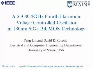
A 2.9-30.3GHz Fourth-Harmonic Voltage-Controlled Oscillator in 130nm SiGe BiCMOS Technology. Yang Lin and David E. Kotecki Electrical and Computer Engineering Department University of Maine, USA. Outline. Voltage-controlled oscillator (VCO) Wide-tuning VCO applications

E N D
A 2.9-30.3GHz Fourth-Harmonic Voltage-Controlled Oscillator in 130nm SiGeBiCMOSTechnology Yang Lin and David E. Kotecki Electrical and Computer Engineering Department University of Maine, USA 17th IEEE International Conference on Electronics, Circuits and Systems
Outline Voltage-controlled oscillator (VCO) Wide-tuning VCO applications Previous work on the state-of-the-art wide-tuning VCOs Design & Post-layout simulation of this work 17th IEEE International Conference on Electronics, Circuits and Systems
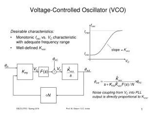
Voltage-Controlled Oscillator (VCO) 17th IEEE International Conference on Electronics, Circuits and Systems
Wide-tuning VCO applications Radar Remote Sensing Broadband Communication 17th IEEE International Conference on Electronics, Circuits and Systems
State-of-the-art wide-tuning VCOs This work The widest tuning range in the 130nm ring VCOs reported 17th IEEE International Conference on Electronics, Circuits and Systems
Architecture • For the XOR, • differential inputs Ap and An (0o delay @ frequency f0 ) • XOR differential inputs Bp and Bn (90o delay @ frequency f0) • = differential outputs Zp and Zn (frequency 2f0 ) • Base-collector-connected (level-shifting) NPN transistors: • decrease the XOR input voltages for Bp and Bn 17th IEEE International Conference on Electronics, Circuits and Systems
Ring Quadrature VCO (QVCO) Delay cell • Gate width/length (µm) • Buffer: Common source (amplified output) • ‘Vctrl’ is high: low-frequency mode, T1 & T4 close to ‘off’, T2 & T3 • provide most currents • ‘Vctrl’ achieves a specific high value, the oscillation freq. keeps the same • ‘Vctrl’ is low: high-frequency mode, |Vgs| of T1 & T4 increases, • current and freq. boost • Increasing ‘Vdd’ boosts the output frequency 17th IEEE International Conference on Electronics, Circuits and Systems
BiCMOS Gilbert XOR Emitter followers as buffers Logic Part Current Source • Logic part, Emitter followers & Current source • Delays of Ap, An, Bp and Bn are 0o, 180o, 90o and 270o • Bp & Bn are ~0.7V lower than Ap & An • Zp and Zn are differential outputs • BiCMOS XOR outperforms CMOS XOR: high freq. & differential outputs • CMOS XOR: up to ~5.5GHz input freq. 17th IEEE International Conference on Electronics, Circuits and Systems
Push-push frequency doubler L Half-circuit model Schematic Half-circuit ( for all x) 17th IEEE International Conference on Electronics, Circuits and Systems
Push-push frequency doubler (continued) L Assuming Zp & Zn out-of-phase: odd harmonics cancel, even harmonics add Doubled frequency dominates !! 17th IEEE International Conference on Electronics, Circuits and Systems
Microchip LayoutSize: 750µm×500µmThe ground & power planes are not shown for clarity. Vbuffer Vdd! Vctrl QVCO Vxor XOR 750µm out Push-push frequency doubler Gnd! VL 500µm 17th IEEE International Conference on Electronics, Circuits and Systems
Post-layout simulation resultsOscillation frequency 30.3GHz Tuning range = 165% 2.9GHz 17th IEEE International Conference on Electronics, Circuits and Systems
VCO transient output at 30.3GHz(into a 50Ω load) •Non-ideal 4th-harmonic output •A small 2nd-harmonic signal still exists due to the incomplete cancellation of Zp and Zn signals •Peak-peak voltage amplitude ~20mV 17th IEEE International Conference on Electronics, Circuits and Systems
4th-harmonic output power spectruminto a 50Ω load 30.3 GHz, -33.5 dBm The rejections 23.5dB @7.575GHz 8dB @15.15GHz 12.5dB @22.725GHz @30.3 GHz, Dissipated power: 34.2 mW, Output power: -33.5 dBm @2.9 GHz, Dissipated power: 32.89 mW, Output power: -56.5 dBm 17th IEEE International Conference on Electronics, Circuits and Systems
Phase Noise (PN) versus offset frequency At 10MHz offset frequency, PN= -86.04 dBc/Hz @ 30.3GHz oscillation frequency PN= -102.2 dBc/Hz @ 2.9GHz oscillation frequency 30.3GHz oscillation frequency, -86.04 dBc/Hz @10MHz offset frequency 17th IEEE International Conference on Electronics, Circuits and Systems
Conclusions 17th IEEE International Conference on Electronics, Circuits and Systems
Thank you very much! 17th IEEE International Conference on Electronics, Circuits and Systems