Versatile Programmable Power Supply for Laboratory Testing and Electronic Devices
This project presents a comprehensive overview of a versatile power supply unit designed for laboratory use and testing of various electronic devices. The unit features multiple outputs, an intuitive user interface including LEDs and LCD displays, and advanced measurement and control capabilities. It employs a dual-loop control scheme utilizing an FPGA for dynamic regulation, integrates DC-DC converters, and supports real-time coefficient adjustments via USB. The design also incorporates system modeling and simulation using MATLAB and Simulink, ensuring optimal performance for diverse electronic applications.

Versatile Programmable Power Supply for Laboratory Testing and Electronic Devices
E N D
Presentation Transcript
HS DSL PowerBench Programmable Power Supply Dror Lazar Moran Fishman Supervisor: Boaz Mizrahi Winter Semester 2009/10
Project Overview - Reminder A versatile power supply unit with multiple outputs for laboratory use and testing of various electronic devices.
סססA brief reminder Project Overview - Reminder User interface D U T Power supply Control unit Measurement unit Active load User interface for standalone operation LEDs LCD Keys
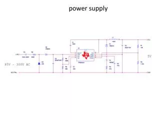
Overview – Control Scheme DAC Output setting DC-DC Converter Post regulator Current Sense Controller Block & Registers Input voltage sense feed- forward PWM Output AuxiliaryVoltage Sense ADC Tempe-rature Current limit ADC Voltage Sense ADC Microprocessor FPGA Cypress FX2 USB Controller USB Cable
FPGA Control Infrastructure • External Loop: Determines VREF input for inner loop : LDO POWER (Pref) = (Vref – Vout) * Iout => VREF = Pref/Iout + Vout implemented using fixed LUT for Pref = 1W Pref LUT Vout Vref Iout
FPGA Control Infrastructure • Internal Loop: Regulates DC-DC converter Implemented using Generic IIR FILTER : 1. Filter order and vectors width determined in FPGA parameter. 2. Filter coefficients determined by software • Enables control design in PC environment (MATLAB) and coefficient streaming to FPGA Control algorithm development without FPGA knowledge • Enables Same FPGA infrastructure for both DC-DCs : Buck & Cuk Converter
Generic IIR Filter • Implementing in FPGA: 1. Filter sample frequency is different from FPGA system frequency (much lower) 2. Sums of many vectors in one clock 2. Consecutive sums & multiples • If IIR filter module is operating in sampling frequency: 1. Low frequency is difficult to create -> unwanted 2. Adds another time domain to the FPGA -> unwanted • Solution : 1. Avoiding direct implementation 2. Adding extra registers between calculative operations
Generic IIR Filter • Twelve 18x18 bit multipliers in FPGA • Allows an order 2 IIR filter
System Modeling • Modeling the plant G(s) for buck & cuk converters in continues time • Translating the continues time model to discrete time model • Determining required control characteristics: Steady state error, Overshoot, settling time Determining desired closed loop poles
System Modeling • Designing the IIR filter in MATLAB • Simulating the system in Simulink • Simulating the system in SPICE ? • Streaming (via USB) different sets of coefficients to FPGA from PC • measuring analog response with scope and comparing results
PC – FPGA communication • PIC software : SPI module (PIC – FPGA) PMP module (PIC – FX2) FPGA soft-reset module • FX2 software : PC enumeration (done by Greg) End-Points configuration Slave-FIFO configuration • Configure FPGA registers using PC : PC => FX2 => PIC => FPGA => PIC => FX2 => PC
FPGA Firmware Updater • PC Firmware Updater:
FPGA Firmware Updater • PC FX2 PIC FPGA • Sending a vendor request to the FX2, setting an interrupt to the PIC • Sending the data from the PC to the Cypress Bulk Endpoint
FPGA Firmware Updater • PC FX2 PIC FPGA • Real Time Operating System is running on the PIC. FX2 interrupt PIC Task activation • Data transfer from the FX2 bulk endpoint to the PIC
FPGA Firmware Updater • PC FX2 PIC FPGA • Data transfer from the PIC to the FPGA’s SPI Flash. • Flash FPGA Firmware download