Download
1 / 8
80 likes | 223 Vues
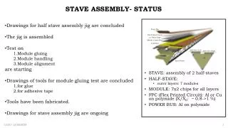
Stave Hybrid Status. Ashley Greenall. Current Status. Current build of hybrids (Version 3) distributed to 6(+1) sites: Cambridge, DESY, Freiburg, LBL, Liverpool and Santa Cruz Glasgow outstanding but pieces available once their jig sets made Used as

E N D
Stave Hybrid Status Ashley Greenall
Current Status • Current build of hybrids (Version 3) distributed to 6(+1) sites: • Cambridge, DESY, Freiburg, LBL, Liverpool and Santa Cruz • Glasgow outstanding but pieces available once their jig sets made • Used as • Mechanicals (gluing studies, wire-bonding) • Leading to electrical test fixtures (DAQ evaluation) • Will ultimately lead to module assembly • Recently received another 60 off circuits stuffed with passives • 59 passed visual • One single failure – solder splash on bond pad • Quality of soldering very good • Electrical performance of hybrids indicates no show stoppers BUT there are features • Identified ‘break’ in Wshunt Disable line on hybrid (affects group of 9 asics in a single column) • Affects operation of PPB slow control on stavelet – no other problems identified • Fix is trivial – requires addition of a single wire bond on a hybrid • Studies of shield-less hybrid show performance is not as expected • See following slides
Shield-less Hybrid Dtnoise at 1fC L1A/COM • Regular pattern seen in Occ. on shield-less hybrid • Affects single (outer) column 0 of hybrid only • Not present on neighbouring column 1 • 2-3 BCOs width • Not seen on shielded type hybrid • Test done using L1A sent down COM line of hybrid Shield-less Hybrid Shielded Hybrid Dtnoise at 1fC using L1A line • L1A now sent down its own dedicated line on hybrid • Now see a different Occ. profile (compared to above) • Again only seen on column 0 • Likewise not seen on shielded hybrid Shield-less Hybrid Shielded Hybrid In both instances this noise profile is not seen when conducting 3PT Gain scans.
Shield-less Hybrid source of the noise • Detailed view of the Dtnoise plots shows discrete • occupancy peaks at differing locations. • For the COM line, 4 discrete peaks per asic location: • Strip pitch is ~75µm, noise peaks are 375µm wide • Corresponds to ~5 channels • Via geometry is 380µm land • Outlying occ. peaks are 20 channels apart, 1.5mm • Outlying via separation is 1.43mm (c-to-c) • Likewise for the L1A line, 3 peaks with similar • geometry profile as above • Outlying occ. peaks are 10 channels apart, 750µm • Outlying via separation is 750µm (c-to-c) • Points to noise injection from the vias • No evidence of pickup from bus traces 1.43mm 750µm 20 channels ~5 channels ~10 channels L1A line COM line
Shield-less Hybrid – why pickup on one column per hybrid Column 0 strips terminate adjacent to opposite column readout asics Clearly passing under the vias Column 1 strips terminate here (at asic edge) • Hybrids are glued onto sensor asymmetrically w.r.t. Sensor strips • Simply done to ensure asic-to-sensor wire bonding geometry is correct • COM & L1A vias are sited directly above the column 0 strips, not the case for column 1 strips • Hence noise injection only seen on the one column of strips
Shield-less Hybrid Performance – Why is it happening? Shield-less Via patterning clearly seen through solder resist Ground + Top layer Patterning is due to asic vacuum holes on FR4 carrier leaving imprint • Power and Ground layers of hybrids have voids around the signal trace vias • Drill span is 1 to 4 i.e. plated-thru-holes through all four layers (done to keep the build simple & cost down) • Vias are not blind – results in them ‘exposed’ on underside (up against sensor) with only glue layer separation • Whereas for the shielded hybrid, bottom shield layer is not perforated – vias are blind up to layer 4 • Shield layer does it’s job – no evidence of pick up with this flavour of hybrid Shielded Via patterning not so obvious Shield + Top layer Solder resist removed to expose Cu of shield layer Fix would be to simply make signal vias (top 2 layers) blind for shield-less hybrid Will result in a non-perforated ground (shield) layer
What next – near term • Planning for a new submission of the hybrid early September • Could go earlier BUT past experience of submitting during vacation time is not good • Hope to get layout files finalised by beginning of August • Will draw up a list of changes would like to take on board for this new submission and circulate • Feedback from users would be useful about changes they would like to see • Known changes are • ‘Fix’ to Wshunt Disable line • Addressing minor issues regarding solder resist - in some cases makes wire-bonding difficult (Problem with BJ820 deep-access head) • Likewise relocate a small number of bond pads • Complete rethink of hybrid cut out tabs – after reflow cause the hybrid edges to rise • Consider also extending the (sacrificial) tabs for module retainment within their frames i.e. glue these to frame • Will re-visit Shield-less hybrid – address signal vias on top 2 layers to make blind • Rigid FR4 former (flex circuit glued to) will revert back to be plated (was not for version 3) – issue with warping • Plating should compensate for the warping • Submission in September should result in hybrid availability late October • Which will then need to go for passive stuffing - expect their availability November
What next – longer term • Preparing for ABC130 – hybrid issues • Proposal is for the topology of hybrid to change from 2 column asic readout to a single column • Assume that this is the default • What level of redundancy will be taken on board • Duplicate CLK/COM buses etc. • Sensor HV spec. • Assume it is 500V + overhead – impacts on layout due to HV clearances • Propose a first attempt at hybrid layout with best guess of uncertainties • Use realistic number of lines (CLK. COM. Data distribution) • ABC130, HCC, Powering asic footprints • Useful exercise as it could be used to feedback optimal locating of asic pad locations • Further material reductions • Number of layers we can get away with and build detail (Kapton/Cu thicknesses etc.) • Use of hatching • Whilst maintaining yield/manufacturability