
Self-Assembled Monolayers in Molecular Nanotechnology
Explore the intricate process and applications of forming self-assembled monolayers with molecular junctions on gold substrates for advanced nanotechnology. Learn about molecular assemblies, nanopatterning, and nanotransfer printing techniques. Dive into the world of molecular nanotechnology.

Self-Assembled Monolayers in Molecular Nanotechnology
E N D
Presentation Transcript
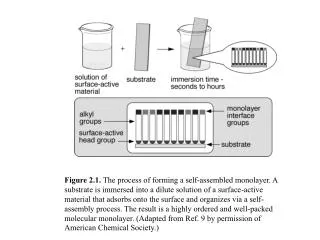
Figure 2.1. The process of forming a self-assembled monolayer. A substrate is immersed into a dilute solution of a surface-active material that adsorbs onto the surface and organizes via a self-assembly process. The result is a highly ordered and well-packed molecular monolayer. (Adapted from Ref. 9 by permission of American Chemical Society.)
Figure 2.2. Schematic representations of an alkanethiolate monolayer on gold. The alkyl chains tilt at a 30 angle from the surface normal, maximizing the inter-chain van der Waals interactions. The sulfur atoms are arranged in a hexagonally close packed formation on the Au(111) surface. The X groups terminating the alkyl chains provide chemical versatility at the monolayer interface. (From Ref. 12 by permission of WILEY-VCH Verlag GmbH & Co.)
Figure 2.3. A schematic representation of Reed and Tour’s molecular junction containing a benzene-1,4-dithiolate SAM that bridges two proximal gold electrodes.(From Ref. 10 by permission of American Association for the Advancement of Science.)
Figure 2.4. (a) Structures of the long and short linked cobalt coordinated terpyridine thiols used as gate molecules. (b) A topographic AFM image of the gold electrodes with a gap. (c) A schematic representation of the assembled single atom transistor.(From Ref. 11 by permission of Macmillan Magazines Ltd.)
Figure 2.5. (a) A schematic representation of the STM patterning of SAMs. (i) Normal STM imaging of the SAM with tip bias Vb; (ii) Removal of SAM by applying a pulse Vp to the gold substrate; (iii) The same as (ii) in solution of conjugated oligomers; (iv) insertion of conjugated oligomers in the patterened sites. (b) STM image of dodecanthiol and conjugated oligomeric patterned SAMs. (i) The STM image after consecutive pulsing at three different locations indicating insertion of molecules (two peaks) and one pit without insertion. (ii) The same region imaged a few minutes later showing adsorption into the remaining pit. (iii) A programmed pattern consisting of circles tracing out a rectangle. (iv) The resulting image of the patterned dodecanthiol SAM after chemisorption of the conjugated oligomers showing the produced rectangular frame. (From Ref. 13 by permission of American Institute of Physics.)
Figure 2.6. Formation of molecular assemblies and corresponding STM images. (a) STM image of diacyl 2,6-diaminopyridine (DAP) decanethiol binder inserted into a surrounding decanthiol monolayer. (b) Image after binding the complementary electroactive Fc-uracil showing an increase in the current-dependent apparent height contrast. (c) “Erased” pattern after replacing the electroactive guest with a more insulating dodecyl functionalized uracil. (From Ref. 14 by permission of American Chemical Society.)
Figure 2.7. (a) Schematic illustration of the CP procedure for patterning an alkanethiol (hexadecanethiol-HDT) on a flat gold substrate. (b) Lateral force microscope (LFM) images (at two different magnifications) of a patterned gold substrate with SAMs terminated in chemically different head groups (HDT-CH3 and16-mercaptohexadecanoic acid-COOH). The image contrast results from differences in frictional forces between the surface and the probe tip. Carboxylic acid terminated SAM show high measured frictional forces (light regions) and methyl terminated SAM show low measured frictional forces (dark regions). (From Ref. 12 by permission of WILEY-VCH Verlag GmbH & Co.)
Figure 2.8. (a) Schematic representation of dip-pen nanolithography (DPN). A water meniscus formed between AFM tip and the gold substrate directs the thiol molecules onto the substrate. The size of the water meniscus is controlled by the relative humidity that in turn affects the overall resolution of DPN. (b) LFM image of an array of octadecanethiol dots on a gold surface generated by holding an ODT-coated AFM tip in contact with the surface for ca. 20 s. (c) LFM image of a molecule-based grid consisting of eight lines 100 nm in width and 2 m in length. (From Ref. 17 by permission of American Association for the Advancement of Science.)
Figure 2.9. (a) Schematic representation of the nanotransfer printing (nTP) procedure to create gold patterns on Si substrates. Optical micrographs of a gold pattern formed by nTP on (b) a silica wafer, and (c) a plastic sheet [organosilsesquioxane modified poly(ethylene terephthalate)], demonstrating the wide applicability of the technique. (From Ref. 18 by permission of American Chemical Society.)
Figure 2.10. (a) The solution-based procedure developed by Brust and Schiffrin for synthesizing alkanethiolate stabilized gold nanoparticles. (b) Schematic illustration showing the curved surface and different regions of a nanopartice SAM.
Figure 2.11. Film growth by the LBL technique: (a) Repeated dipping of a charged-surface slide into polyanion and polycation solutions (steps 1 and 3, respectively) with intermediate washing steps (2 and 4) results in alternate deposition of the corresponding polyions (b). (c) Chemical structures of two typical polyions: sulfonated polystyrene (SPS) and poly(allylamine hydrochloride) (PAH). (From Ref. 25 by permission of American Association for the Advancement of Science.)
Figure 2.12. LBL engineering of a light-emitting device: (a) Multilayer of PPV/PMA performs similarly to PPV alone. (b) Combined architecture of PPV/PMA multilayer on top of PPV/SPS multilayer allows better hole-transport between the PPV/PMA and the ITO anode, and results in enhanced electroluminescence. (From Ref. 32 by permission of American Institute of Physics.)
Figure 2.13. Electrostatic assembly method for creation of functionalized sensing electrodes: alternating deposition steps of (a) negatively charged gold nanoparticles, and (b) positively charged host molecules. Electrodes modified in this fashion with the host shown proved highly sensitive for detection of adrenaline (as the guest molecule). (From Ref. 33 by permission of WILEY-VCH Verlag GmbH & Co.)
Figure 2.14. Polymer capsules: Consecutive adsorption of positively (grey) and negatively (black) charged polyelectrolytes onto negatively charged particles (a,b) and subsequent decomposition of the colloidal core (c,d) yields a suspension of hollow polyelectrolyte capsules (e, TEM image). Addition of crystalline molecules bearing charged groups (f) and changing the ionic or solvent composition drives the molecules into the capsules, where nucleation centers form and crystals are grown. (h) TEM image of a volume-confined crystal of 6-carboxyfluorescein grown inside a capsule that was based on discocyte biocolloid. (From Refs. 35 and 37 by permission of WILEY-VCH Verlag GmbH & Co.)
Figure 2.15. (a) DNA-directed assembly strategy for preparation of network materials from two different-sized oligonucleotide-functionalized nanoparticles. TEM images of: (b) Aggregate formed by linking 8-nm and 31-nm gold nanoparticles, (c) “Satellite” structure obtained in 120-fold excess of the 8-nm colloids. (From Inorg. Chem. 39(11), 2258-2272 (2000) by permission of American Chemical Society and Ref. 41 by permission of American Chemical Society.)
Figure 2.16. (a) Multiple recognition events are translated into nanoparticle aggregate formation. (b) TEM images of spherical aggregates formed at ambient temperature and (c) at –20 °C, showing thermal control over aggregate size. (From Ref. 43 by permission of Macmillan Magazines Ltd.)
Figure 2.17. Schematic illustration of the synthetic routes to homopolymers, random copolymers, and block copolymers.
Figure 2.18. (a) Fundamental differences in phase behavior of different polymers: A blend of two incompatible homopolymer separates into distinct phases on a large scale (left), whereas block copolymers microphase separate into periodic domains on the scale of a single polymer strand (right). (b) Basic morphologies obtained by different block copolymer compositions.
Figure 2.19. Metal nanowire formation using a block copolymer template: Shown are TEM images of: (a) Gold metal vapor-deposited onto a preformed PS-b-PMMA template. (b) After annealing at 180 °C for 1 min., gold nanoparticles segregate selectively to the PS domains and form chains. (c) Repeated deposition and short-time annealing increases the metal loading, forming continuous conductive nanowires. (From Ref. 54 by permission of Macmillan Magazines Ltd.)
Figure 2.20. (a) Schematic of the unit cell of the double gyroid morphology (space group Ia3d) found in certain triblock copolymers of specific block compositions, where the minority component forms three-dimensionally continuous networks of cylinder-like connectors. Selective removal of the PI component of PI-b-P(PMDSS)-b-PI yields: (b) A porous ceramic matrix (for a 24/100/26 kg mole-1 polymer composition, where the PI forms networks), or (c) Silicon oxicarbide strut networks (for a 44/168/112 kg mole-1 composition, where the PI forms the matrix). AFM height images (maximum height 10 nm, high regions appear bright); insets: computer simulations of corresponding volume-rendered surfaces in the double gyroid unit cell. (From Ref. 55 by permission of American Association for the Advancement of Science. )
Figure 2.21. Lithographic mask fabrication from PS-b-PB templates with spherical PB domains. Spherical voids are created by ozonolysis (which degrades the PB into water dispersible fragments), while OsO4 staining increases the PB domain resistance toward etching, and thus negative or positive etching masks are produced. Shown are corresponding TEM images: top: Negative/positive masks that were used to create holes/lines (respectively), where light spots in the left image are voids and dark lines in the right image are stained PB domains; bottom: Transferred patterns on the silicon nitride substrates, where light regions in the left image are ~15-nm-deep etched-out holes in the substrate, and dark regions in the right image are ~15-nm-thick ridges in the substrate, which were protected from etching. (From Ref. 56 by permission of American Association for the Advancement of Science.)
Figure 2.22. High-density nanowire fabrication in a polymer matrix. (a) Array of hexagonally-packed cylinders aligned normal to the substrate is obtained by annealing an asymmetric diblock copolymer above its glass transition under an applied electric field. (b) Cross-sectional TEM image of an 800-nm thick film of PS-b-PMMA on gold after annealing in an electric field of 25 V/m reveals that the PMMA cylinders penetrate all the way through the film. (c) The minor component is degraded and removed, leaving a porous film. (d) Field emission scanning electron microgram (FE-SEM) of PS-b-PMMA thin film after removal of the PMMA cylindrical domains (cross-sectional view). (e) Metal nanowires are grown inside the pores by electrodeposition. (f) SEM image of a fracture surface showing cobalt nanowires partially filling the pores in the block copolymer template. (From Ref. 58 by permission of WILEY-VCH Verlag GmbH & Co and Ref. 59 by permission of American Association for the Advancement of Science.)