VCO Implementation on Printed Circuit Board for Modulation Circuits
Build and design your interface circuit using the provided components. Avoid grounding the DIP switch pins incorrectly. Utilize modulating techniques as needed.

VCO Implementation on Printed Circuit Board for Modulation Circuits
E N D
Presentation Transcript
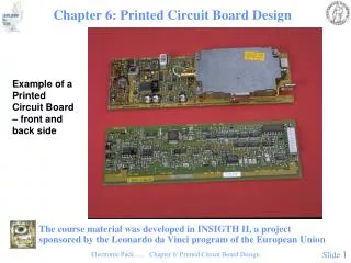
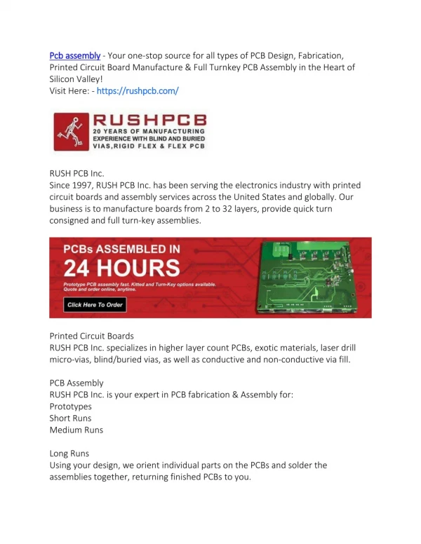
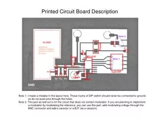
Printed Circuit Board Description Note 2. To VCO Implement whatever interface circuit you need in this area. C2 Crystal C1 R1 Cbypass MC12181 Note 1. Rx Ro Cbypass 8-pin DIP 1000pF CA Cx Co 1000pF GND Note 1. I made a mistake in the layout here. These 4 pins of DIP switch should never be connected to ground, so do not push pins through the holes. Note 2. This part as laid out is for the circuit that does not contain modulator. If you are planning to implement a modulator by modulating the reference, you can use this part: add modulating voltage through the BNC connector and add a varactor or a BJT (as a varactor).