Download
1 / 73
730 likes | 1.02k Vues
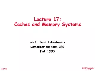
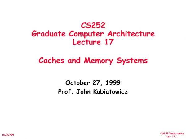
CS252 Graduate Computer Architecture Lecture 17 Caches and Memory Systems. October 27, 1999 Prof. John Kubiatowicz. µProc 60%/yr. 1000. CPU. “Moore’s Law”. 100. Processor-Memory Performance Gap: (grows 50% / year). Performance. 10. DRAM 7%/yr. DRAM. 1. 1980. 1981. 1982. 1983.

E N D
CS252Graduate Computer ArchitectureLecture 17Caches and Memory Systems October 27, 1999 Prof. John Kubiatowicz
µProc 60%/yr. 1000 CPU “Moore’s Law” 100 Processor-Memory Performance Gap:(grows 50% / year) Performance 10 DRAM 7%/yr. DRAM 1 1980 1981 1982 1983 1984 1985 1986 1987 1988 1989 1990 1991 1992 1993 1994 1995 1996 1997 1998 1999 2000 Review: Who Cares About the Memory Hierarchy? • Processor Only Thus Far in Course: • CPU cost/performance, ISA, Pipelined Execution CPU-DRAM Gap • 1980: no cache in µproc; 1995 2-level cache on chip(1989 first Intel µproc with a cache on chip) “Less’ Law?”
What is a cache? • Small, fast storage used to improve average access time to slow memory. • Exploits spacial and temporal locality • In computer architecture, almost everything is a cache! • Registers a cache on variables • First-level cache a cache on second-level cache • Second-level cache a cache on memory • Memory a cache on disk (virtual memory) • TLB a cache on page table • Branch-prediction a cache on prediction information? Proc/Regs L1-Cache Bigger Faster L2-Cache Memory Disk, Tape, etc.
Review: Cache performance • Miss-oriented Approach to Memory Access: • Separating out Memory component entirely • AMAT = Average Memory Access Time
Proc Proc I-Cache-1 Proc D-Cache-1 Unified Cache-1 Unified Cache-2 Unified Cache-2 Example:Harvard Architecture? • Unified vs Separate I&D (Harvard) • Table on page 384: • 16KB I&D: Inst miss rate=0.64%, Data miss rate=6.47% • 32KB unified: Aggregate miss rate=1.99% • Which is better (ignore L2 cache)? • Assume 75% instructions, hit time=1, miss time=50 • Note that data hit has 1 stall for unified cache (only one port) AMATHarvard=75%x(1+0.64%x50)+25%x(1+6.47%x50) = 2.05 AMATUnified=75%x(1+1.99%x50)+25%x(1+1+1.99%x50)= 2.24
Review: Improving Cache Performance 1. Reduce the miss rate, 2. Reduce the miss penalty, or 3. Reduce the time to hit in the cache.
2. Reduce Misses via Higher Associativity • 2:1 Cache Rule: • Miss Rate DM cache size N Miss Rate 2-way cache size N/2 • Beware: Execution time is only final measure! • Will Clock Cycle time increase? • Hill [1988] suggested hit time for 2-way vs. 1-way external cache +10%, internal + 2%
Example: Avg. Memory Access Time vs. Miss Rate • Example: assume CCT = 1.10 for 2-way, 1.12 for 4-way, 1.14 for 8-way vs. CCT direct mapped Cache Size Associativity (KB) 1-way 2-way 4-way 8-way 1 2.33 2.15 2.07 2.01 2 1.98 1.86 1.76 1.68 4 1.72 1.67 1.61 1.53 8 1.46 1.481.47 1.43 161.291.321.32 1.32 32 1.20 1.24 1.25 1.27 64 1.14 1.20 1.21 1.23 128 1.10 1.17 1.18 1.20 (Red means A.M.A.T. not improved by more associativity)
3. Reducing Misses via a“Victim Cache” • How to combine fast hit time of direct mapped yet still avoid conflict misses? • Add buffer to place data discarded from cache • Jouppi [1990]: 4-entry victim cache removed 20% to 95% of conflicts for a 4 KB direct mapped data cache • Used in Alpha, HP machines DATA TAGS One Cache line of Data Tag and Comparator One Cache line of Data Tag and Comparator One Cache line of Data Tag and Comparator One Cache line of Data Tag and Comparator To Next Lower Level In Hierarchy
4. Reducing Misses via “Pseudo-Associativity” • How to combine fast hit time of Direct Mapped and have the lower conflict misses of 2-way SA cache? • Divide cache: on a miss, check other half of cache to see if there, if so have a pseudo-hit (slow hit) • Drawback: CPU pipeline is hard if hit takes 1 or 2 cycles • Better for caches not tied directly to processor (L2) • Used in MIPS R1000 L2 cache, similar in UltraSPARC Hit Time Miss Penalty Pseudo Hit Time Time
5. Reducing Misses by Hardware Prefetching of Instructions & Datals • E.g., Instruction Prefetching • Alpha 21064 fetches 2 blocks on a miss • Extra block placed in “stream buffer” • On miss check stream buffer • Works with data blocks too: • Jouppi [1990] 1 data stream buffer got 25% misses from 4KB cache; 4 streams got 43% • Palacharla & Kessler [1994] for scientific programs for 8 streams got 50% to 70% of misses from 2 64KB, 4-way set associative caches • Prefetching relies on having extra memory bandwidth that can be used without penalty
6. Reducing Misses by Software Prefetching Data • Data Prefetch • Load data into register (HP PA-RISC loads) • Cache Prefetch: load into cache (MIPS IV, PowerPC, SPARC v. 9) • Special prefetching instructions cannot cause faults;a form of speculative execution • Issuing Prefetch Instructions takes time • Is cost of prefetch issues < savings in reduced misses? • Higher superscalar reduces difficulty of issue bandwidth
7. Reducing Misses by Compiler Optimizations • McFarling [1989] reduced caches misses by 75% on 8KB direct mapped cache, 4 byte blocks in software • Instructions • Reorder procedures in memory so as to reduce conflict misses • Profiling to look at conflicts(using tools they developed) • Data • Merging Arrays: improve spatial locality by single array of compound elements vs. 2 arrays • Loop Interchange: change nesting of loops to access data in order stored in memory • Loop Fusion: Combine 2 independent loops that have same looping and some variables overlap • Blocking: Improve temporal locality by accessing “blocks” of data repeatedly vs. going down whole columns or rows
Merging Arrays Example /* Before: 2 sequential arrays */ int val[SIZE]; int key[SIZE]; /* After: 1 array of stuctures */ struct merge { int val; int key; }; struct merge merged_array[SIZE]; Reducing conflicts between val & key; improve spatial locality
Loop Interchange Example /* Before */ for (k = 0; k < 100; k = k+1) for (j = 0; j < 100; j = j+1) for (i = 0; i < 5000; i = i+1) x[i][j] = 2 * x[i][j]; /* After */ for (k = 0; k < 100; k = k+1) for (i = 0; i < 5000; i = i+1) for (j = 0; j < 100; j = j+1) x[i][j] = 2 * x[i][j]; Sequential accesses instead of striding through memory every 100 words; improved spatial locality
Loop Fusion Example /* Before */ for (i = 0; i < N; i = i+1) for (j = 0; j < N; j = j+1) a[i][j]= 1/b[i][j] * c[i][j]; for (i = 0; i < N; i = i+1) for (j = 0; j < N; j = j+1) d[i][j] = a[i][j]+ c[i][j]; /* After */ for (i = 0; i < N; i = i+1) for (j = 0; j < N; j = j+1) { a[i][j] = 1/b[i][j] * c[i][j]; d[i][j] = a[i][j] + c[i][j];} 2 misses per access to a & c vs. one miss per access; improve spatial locality
Blocking Example /* Before */ for (i = 0; i < N; i = i+1) for (j = 0; j < N; j = j+1) {r = 0; for (k = 0; k < N; k = k+1){ r = r + y[i][k]*z[k][j];}; x[i][j] = r; }; • Two Inner Loops: • Read all NxN elements of z[] • Read N elements of 1 row of y[] repeatedly • Write N elements of 1 row of x[] • Capacity Misses a function of N & Cache Size: • 2N3 + N2 => (assuming no conflict; otherwise …) • Idea: compute on BxB submatrix that fits
Blocking Example /* After */ for (jj = 0; jj < N; jj = jj+B) for (kk = 0; kk < N; kk = kk+B) for (i = 0; i < N; i = i+1) for (j = jj; j < min(jj+B-1,N); j = j+1) {r = 0; for (k = kk; k < min(kk+B-1,N); k = k+1) { r = r + y[i][k]*z[k][j];}; x[i][j] = x[i][j] + r; }; • B called Blocking Factor • Capacity Misses from 2N3 + N2 to 2N3/B +N2 • Conflict Misses Too?
Reducing Conflict Misses by Blocking • Conflict misses in caches not FA vs. Blocking size • Lam et al [1991] a blocking factor of 24 had a fifth the misses vs. 48 despite both fit in cache
Summary of Compiler Optimizations to Reduce Cache Misses (by hand)
Summary: Miss Rate Reduction • 3 Cs: Compulsory, Capacity, Conflict 1. Reduce Misses via Larger Block Size 2. Reduce Misses via Higher Associativity 3. Reducing Misses via Victim Cache 4. Reducing Misses via Pseudo-Associativity 5. Reducing Misses by HW Prefetching Instr, Data 6. Reducing Misses by SW Prefetching Data 7. Reducing Misses by Compiler Optimizations • Prefetching comes in two flavors: • Binding prefetch: Requests load directly into register. • Must be correct address and register! • Non-Binding prefetch: Load into cache. • Can be incorrect. Frees HW/SW to guess!
Administrative • Final project descriptions due Monday (11/1)! • Submit web site via email: • Web site will contain all of your project results, etc. • Minimum initial site: Cool title, link to proposal • Anyone need resources? • NOW: apparently can get account via web site • SimpleScalar: info on my web page
Improving Cache PerformanceContinued 1. Reduce the miss rate, 2. Reduce the miss penalty, or 3. Reduce the time to hit in the cache.
1. Reducing Miss Penalty: Read Priority over Write on Miss • Write through with write buffers offer RAW conflicts with main memory reads on cache misses • If simply wait for write buffer to empty, might increase read miss penalty (old MIPS 1000 by 50% ) • Check write buffer contents before read; if no conflicts, let the memory access continue • Write Back? • Read miss replacing dirty block • Normal: Write dirty block to memory, and then do the read • Instead copy the dirty block to a write buffer, then do the read, and then do the write • CPU stall less since restarts as soon as do read
Write buffer:Send writes off to the side CPU in out write buffer DRAM (or lower mem)
2. Reduce Miss Penalty: Subblock Placement • Don’t have to load full block on a miss • Have valid bitsper subblock to indicate valid • (Originally invented to reduce tag storage) Subblocks Valid Bits
3. Reduce Miss Penalty: Early Restart and Critical Word First • Don’t wait for full block to be loaded before restarting CPU • Early restart—As soon as the requested word of the block arrives, send it to the CPU and let the CPU continue execution • Critical Word First—Request the missed word first from memory and send it to the CPU as soon as it arrives; let the CPU continue execution while filling the rest of the words in the block. Also called wrapped fetch and requested word first • Generally useful only in large blocks, • Spatial locality a problem; tend to want next sequential word, so not clear if benefit by early restart block
4. Reduce Miss Penalty: Non-blocking Caches to reduce stalls on misses • Non-blocking cacheor lockup-free cacheallow data cache to continue to supply cache hits during a miss • requires F/E bits on registers or out-of-order execution • requires multi-bank memories • “hit under miss” reduces the effective miss penalty by working during miss vs. ignoring CPU requests • “hit under multiple miss” or “miss under miss” may further lower the effective miss penalty by overlapping multiple misses • Significantly increases the complexity of the cache controller as there can be multiple outstanding memory accesses • Requires multiple memory banks (otherwise cannot support) • Penium Pro allows 4 outstanding memory misses
Integer Floating Point Value of Hit Under Miss for SPEC • FP programs on average: AMAT= 0.68 -> 0.52 -> 0.34 -> 0.26 • Int programs on average: AMAT= 0.24 -> 0.20 -> 0.19 -> 0.19 • 8 KB Data Cache, Direct Mapped, 32B block, 16 cycle miss 0->1 1->2 2->64 Base “Hit under n Misses”
5. Second level cache • L2 Equations AMAT = Hit TimeL1 + Miss RateL1 x Miss PenaltyL1 Miss PenaltyL1 = Hit TimeL2 + Miss RateL2 x Miss PenaltyL2 AMAT = Hit TimeL1 + Miss RateL1x (Hit TimeL2 + Miss RateL2+ Miss PenaltyL2) • Definitions: • Local miss rate— misses in this cache divided by the total number of memory accesses to this cache (Miss rateL2) • Global miss rate—misses in this cache divided by the total number of memory accesses generated by the CPU(Miss RateL1 x Miss RateL2) • Global Miss Rate is what matters
Comparing Local and Global Miss Rates Linear • 32 KByte 1st level cache;Increasing 2nd level cache • Global miss rate close to single level cache rate provided L2 >> L1 • Don’t use local miss rate • L2 not tied to CPU clock cycle! • Cost & A.M.A.T. • Generally Fast Hit Times and fewer misses • Since hits are few, target miss reduction Cache Size Log Cache Size
Reducing Misses: Which apply to L2 Cache? • Reducing Miss Rate 1. Reduce Misses via Larger Block Size 2. Reduce Conflict Misses via Higher Associativity 3. Reducing Conflict Misses via Victim Cache 4. Reducing Conflict Misses via Pseudo-Associativity 5. Reducing Misses by HW Prefetching Instr, Data 6. Reducing Misses by SW Prefetching Data 7. Reducing Capacity/Conf. Misses by Compiler Optimizations
L2 cache block size & A.M.A.T. • 32KB L1, 8 byte path to memory
Reducing Miss Penalty Summary • Five techniques • Read priority over write on miss • Subblock placement • Early Restart and Critical Word First on miss • Non-blocking Caches (Hit under Miss, Miss under Miss) • Second Level Cache • Can be applied recursively to Multilevel Caches • Danger is that time to DRAM will grow with multiple levels in between • First attempts at L2 caches can make things worse, since increased worst case is worse
Main Memory Background • Performance of Main Memory: • Latency: Cache Miss Penalty • Access Time: time between request and word arrives • Cycle Time: time between requests • Bandwidth: I/O & Large Block Miss Penalty (L2) • Main Memory is DRAM: Dynamic Random Access Memory • Dynamic since needs to be refreshed periodically (8 ms, 1% time) • Addresses divided into 2 halves (Memory as a 2D matrix): • RAS or Row Access Strobe • CAS or Column Access Strobe • Cache uses SRAM: Static Random Access Memory • No refresh (6 transistors/bit vs. 1 transistorSize: DRAM/SRAM 4-8, Cost/Cycle time: SRAM/DRAM 8-16
Main Memory Deep Background • “Out-of-Core”, “In-Core,” “Core Dump”? • “Core memory”? • Non-volatile, magnetic • Lost to 4 Kbit DRAM (today using 64Kbit DRAM) • Access time 750 ns, cycle time 1500-3000 ns
DRAM logical organization (4 Mbit) Column Decoder … • Square root of bits per RAS/CAS D Sense Amps & I/O 1 1 Q Memory Array A0…A1 0 (2,048 x 2,048) Storage W ord Line Cell
4 Key DRAM Timing Parameters • tRAC: minimum time from RAS line falling to the valid data output. • Quoted as the speed of a DRAM when buy • A typical 4Mb DRAM tRAC = 60 ns • Speed of DRAM since on purchase sheet? • tRC: minimum time from the start of one row access to the start of the next. • tRC = 110 ns for a 4Mbit DRAM with a tRAC of 60 ns • tCAC: minimum time from CAS line falling to valid data output. • 15 ns for a 4Mbit DRAM with a tRAC of 60 ns • tPC: minimum time from the start of one column access to the start of the next. • 35 ns for a 4Mbit DRAM with a tRAC of 60 ns
DRAM Performance • A 60 ns (tRAC) DRAM can • perform a row access only every 110 ns (tRC) • perform column access (tCAC) in 15 ns, but time between column accesses is at least 35 ns (tPC). • In practice, external address delays and turning around buses make it 40 to 50 ns • These times do not include the time to drive the addresses off the microprocessor nor the memory controller overhead!
DRAM History • DRAMs: capacity +60%/yr, cost –30%/yr • 2.5X cells/area, 1.5X die size in 3 years • ‘98 DRAM fab line costs $2B • DRAM only: density, leakage v. speed • Rely on increasing no. of computers & memory per computer (60% market) • SIMM or DIMM is replaceable unit => computers use any generation DRAM • Commodity, second source industry => high volume, low profit, conservative • Little organization innovation in 20 years • Order of importance: 1) Cost/bit 2) Capacity • First RAMBUS: 10X BW, +30% cost => little impact
DRAM Future: 1 Gbit DRAM (ISSCC ‘96; production ‘02?) Mitsubishi Samsung • Blocks 512 x 2 Mbit 1024 x 1 Mbit • Clock 200 MHz 250 MHz • Data Pins 64 16 • Die Size 24 x 24 mm 31 x 21 mm • Sizes will be much smaller in production • Metal Layers 3 4 • Technology 0.15 micron 0.16 micron
Main Memory Performance • Simple: • CPU, Cache, Bus, Memory same width (32 or 64 bits) • Wide: • CPU/Mux 1 word; Mux/Cache, Bus, Memory N words (Alpha: 64 bits & 256 bits; UtraSPARC 512) • Interleaved: • CPU, Cache, Bus 1 word: Memory N Modules(4 Modules); example is word interleaved
Main Memory Performance • Timing model (word size is 32 bits) • 1 to send address, • 6 access time, 1 to send data • Cache Block is 4 words • Simple M.P. = 4 x (1+6+1) = 32 • Wide M.P. = 1 + 6 + 1 = 8 • Interleaved M.P. = 1 + 6 + 4x1 = 11
Independent Memory Banks • Memory banks for independent accesses vs. faster sequential accesses • Multiprocessor • I/O • CPU with Hit under n Misses, Non-blocking Cache • Superbank: all memory active on one block transfer (or Bank) • Bank: portion within a superbank that is word interleaved (or Subbank) … Superbank Bank Superbank Offset Superbank Number Bank Offset Bank Number
Independent Memory Banks • How many banks? number banks number clocks to access word in bank • For sequential accesses, otherwise will return to original bank before it has next word ready • (like in vector case) • Increasing DRAM => fewer chips => harder to have banks
32 8 8 2 4 1 8 2 4 1 8 2 DRAMs per PC over Time DRAM Generation ‘86 ‘89 ‘92 ‘96 ‘99 ‘02 1 Mb 4 Mb 16 Mb 64 Mb 256 Mb 1 Gb 4 MB 8 MB 16 MB 32 MB 64 MB 128 MB 256 MB 16 4 Minimum Memory Size
Avoiding Bank Conflicts • Lots of banks int x[256][512]; for (j = 0; j < 512; j = j+1) for (i = 0; i < 256; i = i+1) x[i][j] = 2 * x[i][j]; • Even with 128 banks, since 512 is multiple of 128, conflict on word accesses • SW: loop interchange or declaring array not power of 2 (“array padding”) • HW: Prime number of banks • bank number = address mod number of banks • address within bank = address / number of words in bank • modulo & divide per memory access with prime no. banks? • address within bank = address mod number words in bank • bank number? easy if 2N words per bank
Fast Bank Number • Chinese Remainder TheoremAs long as two sets of integers ai and bi follow these rules and that ai and aj are co-prime if i j, then the integer x has only one solution (unambiguous mapping): • bank number = b0, number of banks = a0 (= 3 in example) • address within bank = b1, number of words in bank = a1 (= 8 in example) • N word address 0 to N-1, prime no. banks, words power of 2 Seq. Interleaved Modulo Interleaved Bank Number: 0 1 2 0 1 2Address within Bank: 0 0 1 2 0 16 8 1 3 4 5 9 1 172 6 7 8 18 10 2 3 9 10 11 3 19 11 4 12 13 14 12 4 20 5 15 16 17 21 13 5 6 18 19 20 6 22 14 7 21 22 23 15 7 23
Fast Memory Systems: DRAM specific • Multiple CAS accesses: several names (page mode) • Extended Data Out (EDO): 30% faster in page mode • New DRAMs to address gap; what will they cost, will they survive? • RAMBUS: startup company; reinvent DRAM interface • Each Chip a module vs. slice of memory • Short bus between CPU and chips • Does own refresh • Variable amount of data returned • 1 byte / 2 ns (500 MB/s per chip) • Synchronous DRAM: 2 banks on chip, a clock signal to DRAM, transfer synchronous to system clock (66 - 150 MHz) • Intel claims RAMBUS Direct (16 b wide) is future PC memory • Niche memory or main memory? • e.g., Video RAM for frame buffers, DRAM + fast serial output