Download
1 / 14
140 likes | 311 Vues
Instrumentation for High Energy Particle and Nuclear Physics. Schematics of 3D (Sandaker). Proposed by S.I. Parker, C.J. Kenney and J. Segal (NIM A 395 (1997) 328)

E N D
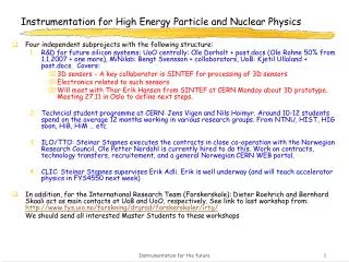
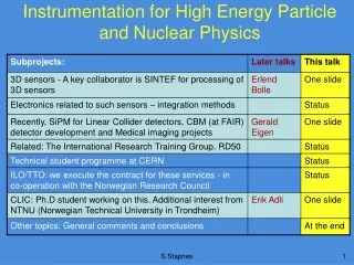
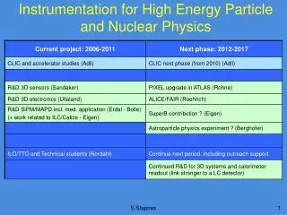
Instrumentation for High Energy Particle and Nuclear Physics S.Stapnes
Schematics of 3D (Sandaker) • Proposed by S.I. Parker, C.J. Kenney and J. Segal (NIM A 395 (1997) 328) • Called 3-D because, in contrast to silicon planar technology, have three dimensional (3-D) electrodes penetrating the silicon substrate • SINTEF/UiO are currently processing 3D structures for a group consisting investigation by a collaboration within Brunel Univ., Hawaii Univ., Stanford Univ. and CERN – batch two expected this year - Depletion thickness depends on p+ and n+ electrode distance, not on the substrate thickness (1) can operate at very low voltages, (2) can have a high doping for ultra-high radiation hardness, (3) are fast and (4) can be active almost to the edge S.Stapnes
Combining electronics and sensors (Ullaland) • Motivation to develop a new pixel detector • Radiation hardness improvement (leakage, reverse annealing issues) • Decrease fabrication cost of pixel detector • Develop a thin pixel detector • Easy fabrication of large area devices • Overcome readout limitation’ • Some concepts of silicon pixel detectors in HEP on the right (more possible) Hybrid pixel DEPFET pixel MAPS S.Stapnes
High Power consumption Low Power consumption Short Connection Long Connection Low Density High Density Poor Heat Dissipation Good Heat Dissipation RC Delays Reduced RC Delays High Impedance Low Impedance Source : Fraunhofer-IZM Large Area Smallest Area James Lu, RPI, Peaks in Packaging, 2003 Challenging Interposers Simple Interposers Less I/O Pitch limitations I/O Pitch limitations Industry Vision 3D will be used for: memories (memory cards), optical sensors (CMOS), smart cards
Photo-readout – SiPM (Erdal, Bolle)(see also talk of Eigen) Resistor Rn= few MΩ • Silicon photomultipliers are semiconductor photon sensitive devices build from an avalanche photodiode matrix on common silicon substrate: • B-field proof, small, good timing resolution, affordable • Total quantum efficiency similar to a traditional PMT • Gain (G) is also similar to a PMT, G vs Vb curve is linear • Dimensions permits extremely compact, light and robust mechanical design • Being explored in many applications today – many companies offering various types – including medical field • Lot of work ahead to understand for example radiation tolerances and operational parameters Depletion Region R 50 substrate ND280 has chosen to use MPPC as the photosensors for all scintillator detectors. – Need ~50,000 MPPCs for ND280; first large-scale use of these devices Pixel size: ~25 x 25 mm2 to ~100 x 100 mm2 Array size: 0.5 x 0.5 mm2 to 5 x 5 mm2 Hamamatsu MPPC Active area: 1.3x1.3 mm2 Number of pixels: 667
Accelerator physics – CLIC – Ph.D student from 1.7.2006 (Adli) • The Ph.D project of Erik Adli is finishing this year, and we seeking ways to continue this very successful initial project. • Specifically, Erik Adli – who will present the status and future plans for this work - will apply for a post.doc position • We have also submitted a Nordic application for funds (NorduCLIC) with partners in Uppsala and Helsinki. S.Stapnes
ILO and TTO – Technical Students (Nordahl) • The work of the Industry Liaison and Technology Transfer Officer Ole Petter Nordahl will be presented by him • The Norwegian Technical student program is currently very successful. • From an initial investment of support for 3-4 months the students are typically extended by CERN to 12 months, and even 14 months in some cases. The monthly cost is 3414 CHF, i.e 17750 NOK. • The two Norwegian CERN staff members who have been doing most of the work have been Jens Vigen and Nils Høimyr, and they are willing to continue to promote the program. Jens Vigen leads the sub-project. • We are now focusing on five areas for these students (but not exclusively) – areas where we have Norwegian activities and/or staff (order arbitrary): • Technology Transfer • Information Technology • Information Systems • CLIC and accelerator technology • Silicon sensors and electronics S.Stapnes
International Research Training Group = Forskerskole • Excellent student training/education • Regular workshops (financed outside this project) • Successfully reviewed in Sept 2008 in Heidelberg • Norwegian funding determine the output from this activity from our side – remains limited S.Stapnes
Objectives and status - I • Join forces to develop challenging new silicon technology taking advantage of knowledge base and new infrastructure in Norway. • For 3D sensors the work is progressing well but there are still concerns about industrial availability of such sensors, and further lab and testbeam measurements are needed. • The SiPM/MAPD work that was only mentioned briefly in the initial application has been successfully strengthened trough international collaborations and small local infrastructure funding. • Extra funding is now available linked to development of a PET demonstrator in Oslo. • Focus on basic technology development the first three years, related to 3D silicon sensors and new integration methods for sensors and electronics. • As mentioned 3D sensor work is making good progress and can move into a stage of preparing for construction projects – for example LHC upgrades, while the work on integration methods clearly will take longer. The MAPS technology is fairly well developed and Norwegian involvement in this area, even if limited, is clearly interesting. • Include a large number of students, in silicon detector system research using fully the link to “Forskerskole” students. • The school has been evaluated successfully in Germany in September 2008, but there is limited funding on the Norwegian side in this area so our participation is still not as strong as it could have been. S.Stapnes
Objectives and status - II • Establish a new ILO and TT system where the focus is longer term and on technology transfer and knowledge, via projects and human resources spending time on CERN, in addition to the traditional CERN contract follow up. • This is going well. • Strengthen the technical students program, and co-ordinate training of Norwegian students to provide an overall consistent environment for them where there is increased contact between the students, Norwegian CERN staff and researchers, and Norwegian Industries being involved in CERN projects. • The actual program is going well in terms of number of students and with good quality, but the connection between Norwegian R&D activities and the technical student program can still be improved. • Participate in CLIC accelerator research to have a minimal activity in accelerator research, and also to answers CERN request for voluntary contributions to CLIC. • This project is going well and the focus now is on finding a longer term funding for the CLIC participation. A Norwegian technical student is now also involved, and an additional Ph.D grant is awarded for LHC accelerator studies. S.Stapnes
Next period Adv. Instrumentation (green, plus yellow?) S.Stapnes
Funding, People • Funding being used within a revised profile with some small adjustment between 2008-2010, keeping the total constant • Basically only funding for 3D sensors and lab equipment planned – so ok for 3D sensors • SiPM/MAPD solutions found outside • ILO/TTO, GRID, and Technical students executed according to plans and budgets S.Stapnes
Test chip • Developed by Einar Nygaard, Interon AS here in Oslo for us • Analogue low noise readout for pixel sensors • Will use to study: • Sensor performance • Sensors after SLID bonding • System performance after applying via process • Our goal: to apply with 3D sensors making modules active all the way to edge S.Stapnes