CIC-310 CPLD/FPGA Development System
K&H MFG. Co., LTD . Manufacturer, Exporter & Importer for Educational Equipment & Measuring Instrument. CIC-310 CPLD/FPGA Development System. CIC-310 CPLD/FPGA Development System. § CPLD / FPGA Background. § Hardware Overview --- System Overview --- Development Board

CIC-310 CPLD/FPGA Development System
E N D
Presentation Transcript
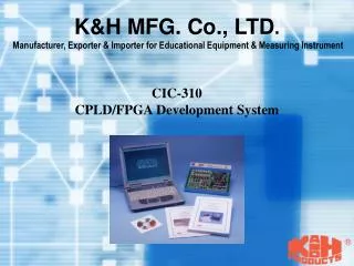
K&H MFG. Co., LTD. Manufacturer, Exporter & Importer for Educational Equipment & Measuring Instrument CIC-310 CPLD/FPGA Development System
CIC-310 CPLD/FPGA Development System §CPLD / FPGA Background §Hardware Overview --- System Overview --- Development Board --- Experiment Board §Design Flowchart --- Experiment Flowchart --- Programming Flowchart --- Program manager §Experiments --- List of experiments --- Implementations
CIC-310 CPLD/FPGA Development System §CPLD / FPGA Background §Hardware Overview --- System Overview --- Development Board --- Experiment Board §Design Flowchart --- Experiment Flowchart --- Programming Flowchart --- Program manager §Experiments --- List of experiments --- Implementations
Manual Truth table Manual (K-map) Boolean expression X = (Ā+B+C) (B+D) ( Ā+D ) Manual Implement on several ICs §CPLD/FPGA BACKGROUND – (1) Traditional design flow of the logic circuit Design specification In = A, B, C, D ... Out = X, Y …
A B C Programmable switch or fuse AND plane PAL – Programmable Array Logic Programmable AND array followed by fixed fan-in OR gates
A B C PLD A D Q Q B C D S0 Q S1 AND plane PLD - Programmable Logic Device HDL : Hardware Description Language
I/O Block PLD Block PLD Block I/O Block Interconnection Matrix Interconnection Matrix I/O Block PLD Block PLD Block I/O Block CPLD (Complex PLD) Structure Integration of several PLD blocks with a programmable interconnect on a single chip
LUT A B Z A C D B Z C D FPGA Look-Up Tables (LUT) • Look-up table with N-inputs can be used to implement any combinatorial function of N inputs • LUT is programmed with the truth-table LUT implementation Truth-table Gate implementation
FPGAs vs. CPLDs • Are FPGAs and CPLDs the same thing? No. Both are programmable digital logic chips. Both are made by the same companies. But they have different characteristics. • FPGAs are "fine-grain" devices. That means that they contain a lot (up to 100000) of tiny blocks of logic with flip-flops. CPLDs are "coarse-grain" devices. They contain relatively few (a few 100's max) large blocks of logic with flip-flops. • FPGAs are RAM based. They need to be "downloaded" (configured) at each power-up. CPLDs are EEPROM based. They are active at power-up (i.e. as long as they've been programmed at least once...). • CPLDs have a faster input-to-output timings than FPGAs (because of their coarse-grain architecture, one block of logic can hold a big equation), so are better suited for microprocessor decoding logic for example than FPGAs. • FPGAs have special routing resources to implement efficiently binary counters and arithmetic functions (adders, comparators...). CPLDs do not. • FPGAs can contain very large digital designs, while CPLDs can contain small designs only.
FPGA & CPLD • FPGAs are RAM based. They need to be "downloaded" (configured) at each power-up. CPLDs are EEPROM based. They are active at power-up (i.e. as long as they've been programmed at least once...). • FPGAs can contain very large digital designs, while CPLDs can contain small designs only. • CPLDs have a faster input-to-output timings
Manual (programming) Design description HDL Syntax Automatic Implement on ONE CPLD/FPGA chip §CPLD/FPGA BACKGROUND – (2) Modern design flow of the logic circuit Design specification In = A, B, C, D ... Out = X, Y … Save lots of time!!!
MCU MPU Decoder PWM Converter Memory ALU Counter GPIO Control Timer SOPC(System On Programmable Chip) FPGA/CPLD
CIC-310 CPLD/FPGA Development System §CPLD / FPGA Background §Hardware Overview --- System Overview --- Development Board --- Experiment Board §Design Flowchart --- Experiment Flowchart --- Programming Flowchart --- Program manager §Experiments --- List of experiments --- Implementations
§System Overview CIC-310 CPLD/FPGA Development Board Experiment Board + = CIC-310 provides digital system designers with an economical solution for hardware verification or students with an efficient learning of digital system design.
§Hardware Overview – Development Board 89C2051 for load the configuration data to FPGA or SEEPROM devices with data compression techniques HIN230 for RS-232 transmitters/receivers interface circuits Reset button: Reset connection to PC Program selector jumper 11.0592MHz Xosc Altera 8k/10k RAM-based FPGA RS232 connector Max. 32kBSEEPROM 7.5C DC Power
§Hardware Overview – Experiment Board 16-Segment Display Section 6-Digit Parallel-Serial 7-segment Display Output Logic LED Display 20MHz X’TRAL OSC 5 x 7 DOT LED display RC Oscillator Logic Switch Input Section SW and Keypad Section Pulse generator Input Status Logic LED Display
CIC-310 CPLD/FPGA Development System §CPLD / FPGA Background §Hardware Overview --- System Overview --- Development Board --- Experiment Board §Design Flowchart --- Experiment Flowchart --- Programming Flowchart --- Program manager §Experiments --- List of experiments --- Implementations
Experiment Board Show the result §EXPERIMENT FLOWCHART Windows 98/2000/XP Personal Computer Programming Rs-232 Development Board Download the program Program manager
§Program manager functions Add the program to SEEPROM Execute the program from SEEPROM Download the program to FPGA and execute the program
CIC-310 CPLD/FPGA Development System §CPLD / FPGA Background §Hardware Overview --- System Overview --- Development Board --- Experiment Board §Design Flowchart --- Experiment Flowchart --- Programming Flowchart --- Program manager §Experiments --- List of experiments --- Implementations
§LIST OF EXPERIMENTS • Combinational logic circuits • Applications of ALUs • Encoder / Decoder • Alpha-Nemaric LED display • Multiplexer / Demultiplexer • Sequential logic circuits • Flip-flop circuits • Applications of counters • Frequency synthesizers / Shift Registers • Dynamic 5x7 LED matrix display • 4x4 keypad of matrixes More than 50 examples in the experimental manual!!!
Implementations Exp1 : Step by step design of basic logic circuit by Graphic and Text Editor Exp2 : Binary-to-16-segment decoder Exp3: Counters Exp4: 5X7 DOT matrix display Exp5: Keypad
Exp1: Basic logic circuit design (Primal.gdf) Specification: Output : P55, P56, P57, P58 Input: DIP switches Output: LED display Relation: P55 = !P01 P56 = P02 & P03 P57 = P04 # P06 P58 = P07 $ P08 ! => NOT & => AND # => OR $ => XOR Input: P01, P02, P03, P04, P06, P07, P08
Step 1: Programming by graphic editor P01 P55 P02 P56 P03 P04 P57 P06 P07 P58 P08
Step 2: Assign Devices (Assign / Devices) Step 3: Save&Compile (Max+Plus II / Compiler)
Step 4: Simulation ( 1. Max+Plus II / Waveform Editor ) ( 2. Max+Plus II /Simulator)
Step 5: Download the program Add the program to SEEPROM Download the program to FPGA and execute the program Execute the program from SEEPROM
Program by Text Editor --- Primal.tdf The rest design steps are the same
Exp2: Binary-to-16-segment decoder Specification: Output : 16-segment display Input: DIP switches Output: 16-segment display Relation: 6 bit inputs are decoded to 16-segment display as: Numerical number : 0~9 Alphabet letters : A~Z Math Operators: *,+,-,/ Why you need 6-bit input? Input: P01, P02, P03, P04, P06, P07 0~9 10 A~Z 26 *,+,-,/ 4 10+26+4=40 2^6 = 64 > 40
. . . Program by Text Editor --- 16segb.tdf Symbol Position
Pin Assignment (1) 2 1 Table 1-6 16 segment display pin-out (8k-84pin)
P13 P14 P24 P27 P29 P15 P21 P22 P23 P28 P30 P20 P25 P16 P63 P19 P18 Pin Assignment (2) Symbol Segment Pin
Show Result FPGA JP8 JP9 JP10 JP8 JP9 JP10 FPGA Pin Symbol
Exp3: Counters Specification: Output : P55, P56, P57, P58 Construct a 4-bit asynchronous counter by T flip-flops Input: Enable: Sw1_1 Reset: Sw1_2 Clock: SWP3 Output: LED display Relation: The 4-bit ripple counter repeats itself for every 2^4 (16) clock pulses.: Input: Sw1_1, p01 (Enable) Sw1_2, P02 (Reset) SWP3, P83 (Clock)
Asynchronous Counter:Program by Graphic Editor --- 4slcnt.gdf
Asynchronous Counter:Program by Text Editor --- 4slcnt.gdf TFF primitive
Asynchronous Counter:Program by Text Editor --- 4slcnt.gdf FF[]=FF[]-1;
Synchronous Counter:Program by Graphic Editor --- ptcnt8.gdf
Delay Matrix Asynchronous Counter Synchronous Counter
4 Digit Counter:Frequency Counter --- pdec9999.tdf Input: Clock Output: LED Display (Counting 0~9999 in binary format)
7 segment displayer --- 7segd.tdf Input: DIP switch Output: 7 segment displayer SA SB SC SD SE SF SG
0 0 0 1 1 1 2 2 2 3 3 3 4 4 4 5 5 5 6 6 6 7 7 7 8 8 8 9 9 9 4 Digit Counter:Parallel mode --- 4dec7sp.tdf Require Pins: 6 x 4 = 24
4 Digit Counter:Serial Scan mode --- 4dec7sn.tdf Require Pins: 6 x 1 + 4 = 10 0 1 0 2 0 3 4 5 0 0
P13 PA1 P14 PA2 P15 PA3 P16 PA4 PA5 P18 PA6 P19 PA7 P20 P22 P23 P24 P25 P27 Exp4: 5x7 dot matrix display 5x7 Matrix DOT display (dot_test.tdf)
1 P13 PA1 P14 PA2 P15 PA3 P16 PA4 PA5 P18 PA6 P19 PA7 P20 P22 P23 P24 P25 P27 0 5x7 DOT Matrix display (dot_test.tdf) 1 0 1 0 1 Counter TRY 57dots.hex !!!
P48 P43 P34 P39 P49 P44 P35 P40 P50 P45 P36 P41 P51 P46 P37 P42 Exp5: Keypad Individual Mode --- require 16 ports Parallel Mode => PKI1, PKI2, PKI3 Serial Mode => SCN1, SCN2, SCN3 Scan Mode --- require 8 ports

