Understanding Combinational Logic Design: Positive vs. Negative Logic Procedures
This article delves into the principles of combinational logic design, focusing on the distinction between positive and negative logic systems. It explains how signal levels are assigned to logic values in both systems, emphasizing their implications in circuit design. The design procedure parallels software development and covers specification, formulation, optimization, mapping, and verification. Furthermore, real-world design examples highlight the application of these concepts, including the design of BCD-to-Excess-3 converters and 4-bit equality comparators, offering a comprehensive guide to effective combinational design.


Understanding Combinational Logic Design: Positive vs. Negative Logic Procedures
E N D
Presentation Transcript
Topics • Positive vs. negative logic • Design procedure
Positive and Negative Logic Two different assignments of signal levels to logic values are possible • Using H level to represent a logic 1 (true) defines a positive logic system • Using H level to represent a logic 0 (true) defines a negative logic system
AND Gate Specification • IC data sheets define gates in terms of both signal values and logic values • Example: physical behavior specification of a CMOS gate • What is the logic function implemented by this gate ??
a polarity indicator: signify that NEGATIVE LOGIC is assumed for the signal Positive vs. Negative Logic
Bottom Line • Not much real change • Negative logic functions are just duals of positive logic ones • AND -> OR • OR -> AND
Design Procedure Similar to software • Specification – problem description • Write a specification for the circuit • Formulation – as truth table, Boolean function, or ( Verilog: in Lab) • define the required relationships between inputs and outputs • Optimization – used to be manual, now CAD tool • Draw a logic diagram or provide a netlist for the resulting circuit (AND, OR, INVERTORS) • Mapping – to select the implementation technology • Transform the diagram or netlist to a new diagram or netlist using the available implementation technology • Verification – used to be manual, now simulation • Verify correctness of design
2. Formulation 3. Optimization 4. Mapping Example 1 • Specification:3 binary inputs; Output is 1 when input < 011
5. Verification • Verify correctness of design • Manual: perform analysis of circuit • Simulation
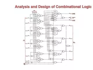
Analysis of Circuit • Used in manual design verification and other purposes • This shows a disciplined way to analyze a circuit • To get Boolean function • and/or Truth table
Derivation of Func. Or Table • Label gate outputs in terms of “input variables” • Determine Boolean functions or values • Label outputs of gates fed by previously labeled gates • Determine Boolean function or values • Repeat 2 until done
Derivation of Truth Table • Make table with 2n rows, where n is number of inputs • Label some gate outputs • Put those labels and the final outputs on columns of truth table • Work your way across
Design Examples • Design Examples in the book • Study on your own: • Example 3-1 (p.99) : Design of a BCD-to-Excess-3 Converter • Example 3-2 (p.101) : Design of a BCD-Seven-Segment Decoder • Examples 3-3 (Will do in class) : Design of a 4-bit Equality Comparator • Input: 2 vectors A(3:0) and B(3:0) • Output: One bit, E, which is 1 if A and B are bitwise equal, 0 otherwise
Design of a 4-bit Equality Comparator • Specification : • Input: 2 vectors A(3:0) and B(3:0) • Output: One bit, E, which is 1 if A and B are bitwise equal, 0 otherwise • Hierarchical design seems a good approach • One module/bit • Final module for E
Design for MX module • Logic function Ei=0 if Ai and Bi have the same value; Ei = 1 if Ai and Bi have different values • Can implement as
Design for ME module • Final E is 1 only if all intermediate values are 0 • So • And a design is