
Horz
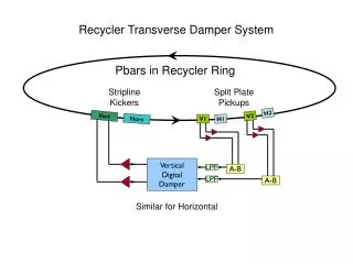
Recycler Transverse Damper System. Pbars in Recycler Ring. Stripline Kickers. Split Plate Pickups. H2. Vert. V2. Horz. V1. H1. Vertical Digital Damper. LPF. A-B. LPF. A-B. Similar for Horizontal. V1 Digital Damper. Boards used for MI Damper systems

Horz
E N D
Presentation Transcript
Recycler Transverse Damper System Pbars in Recycler Ring Stripline Kickers Split Plate Pickups H2 Vert V2 Horz V1 H1 Vertical Digital Damper LPF A-B LPF A-B Similar for Horizontal
V1 Digital Damper • Boards used for MI Damper systems • Standalone board with on board cpu (Sharc) & ethernet – communicates with ACNET via OAC • Four boards are operational • 2 for MI dampers, 1 for Recycler Damper, 1 being used for Booster damper studies • A 5th board exists but was never made operational • At present, the Booster board can be considered spare hardware – work is needed to actually make it into a spare for any of the operational systems • Operational since fall 2005 with no major hardware/system issues Implemented in one FPGA based damper board developed by B. Foster & A. Seminov
V1 Damper Block Diagram Peak Detector & RMS Readback by ACNET 4 Sample Boxcar Filter ADC Input DAC Output Box X X Delay Delay + - Input Gain Output Gain 212MHz 212MHz 1 Turn Invert DAC Output ADC Input Box X Delay Delay Notch Filter Peak Detectors Readback by ACNET • System Bandwidth is determined by analog LPF on inputs • Programmable delay is limited to 212MHz clock rate (1/4 RF bucket)
V1 Damper Amplitude and Phase Response • Phase has been inverted so that 0° is damping • The analog 30MHz LPF causes phase shift as it rolls off the gain • The system goes unstable at ~37Mhz once the Beam Density reaches about 2.5
V2 Digital Damper • Developed as next generation replacement for the “Foster” Board • VME format to take advantage of standard controls software • Interface implemented in FPGA • Remove Sharc processor • Same basic design with updated FPGA and Digital to Analog Converters • Applied lessons learned on V1 design to take better advantage of FPGA features • 15 boards have been assembled • Used for Recycler RF Adaptive Correction • Used for Recylcer ACBEAM intensity Monitor • Used for MI Anti-proton Damper • Plan to replace MI Proton Dampers • 8 spares available
V2 Recycler Damper • Faster DACs and next generation FPGA allow us to double the system bandwidth and increase performance • Standard Controls ACNET interface implemented in VME processor • Use extra channels for Testing & Diagnostics • Network analyzer can be hooked up to spare channels for transfer function measurements • Can make both open loop measurements without changing cables on operational system • Can also make closed loop measurements Use 2 VME boards -1 per plane
V2 Damper Block Diagram Peak Detector & RMS Readback by ACNET 8 Tap FIR Filter ADC Input DAC Output FIR X X Delay Delay + - Input Gain Output Gain 212MHz 636MHz 1 Turn Invert DAC Output ADC Input FIR X Delay Delay Notch Filter Peak Detectors Readback by ACNET • System Bandwidth is controlled by FIR filter with constant phase • the analog anti-alias filter is upped to 70MHz • Programmable delay possible at 636MHz clock rate (1/12 RF bucket) • This allows increased system bandwidth to improve performance
V2 Damper Amplitude and Phase Response • Phase has been inverted so that 0° is damping • The analog 70MHz Filter does not affect the phase until about 60MHz • System gain is controlled with programmable FIR filter • The system goes unstable >70MHz once the Beam Density is > 4
Brief V2 History • First issue was with analog input circuit to the ADC • Modified circuit to improve signal termination • 1st modification was susceptible to a failure due to poor solder joint which caused 7.5MHz resonance • Has been fixed • Remaining issues have all been caused by timing issues within the FPGA design • Fixed logic which handles ADC/DAC data • Found and eliminated temerature dependence in FPGA PLL clocks – was causing delay shifts in design • Latest issue appears due to rare (1 second/50 hours) timing glitch within the digital filter logic • Only present in Horz board whose FPGA runs hotter due to crate • Horizontal VME slots and poor air flow • This is a product of the most recent design – not observed before 12/07 • Note that marginal timing issues are sensitive to temperature & power
Installation on 3/18/08 • While preparing to switch that morning, Vertical board spontaneously performed a firmware reload from flash memory • Made decision to abort the switch • Never observed before • FPGA lost design – power glitch? • Glitch on VME_SysReset*? • Has not happened again… • Horizontal Board had PLL losing lock that afternoon • Clock input was swapped and moved to Z crate • Removed from MI60 and put in teststand – fine since…
Installed on 4/23/08 • Found blown fuse on Reset Card • VME_SysReset* on backplane was 2V • Updated Design to be less sensitive to glitches on VME_SysReset* • Require signal to be low for >200ns • No further spontaneous resets observed for 3+ weeks of monitoring • Made request to install
Initial Results Good • Attempted to induce instability with 80e10 • Density reached ~3.5 • No instability • Measured closed loop response during test • Looked good
Clock PLL Event on 5/1/08 • Vertical Damper Turned Off when it’s RF PLL lost lock • Got an immediate vertical instability • The Vertical Damper in the test crate also turned off • Jim & I were both at MI60 at the time looking into scope and network analyzer issues
The Suspects • Power • Hard to imagine this just hitting 1 of 2 boards in 2 different crates • The crates are on completely separate circuits • Temperature • Known temperature issues with FPGA and PLL • Found Fan on Operational Vertical board was stopped but Test Vertical was fine • Noise/Problem with Clock • Could not see how only 2 of 4 boards would lose lock
Temperature • Installed Temperature monitors and new fanpacks • Did not see any Events or temperature correlation
Started Looking at Noise • On 5/5 saw 4 glitches in 1 hour while poking around at MI60 • All recent glitches (last few months) occurred when someone was at MI60 • Discovered Cell phone activity at 800-900Mhz was coupling into clock circuit and causing PLL to lose lock • Able to reproduce reliably in teststand • Looking at circuit on NA showed high impedance from 700Mhz to 1GHz
Clock Improvements • Implemented filters and shielding to eliminate high frequency noise from the clock input circuit • No longer see PLL glitches from cell phone or 1Watt RF antenna • Also implemented state machine to provide best recovery scenario should the PLL briefly lose lock in the future
Summary • Have identified cause for PLL to lose lock • Last few “glitches” now completely understood • Have a very plausible root cause for the timing issues which have plagued the system for the last 6 months • The VME Dampers are now back in operation