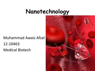
Nanotechnology
Nanotechnology. Nanotechnology definition (NSET, February 2000).

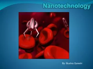
Nanotechnology
E N D
Presentation Transcript
Nanotechnology definition (NSET, February 2000) Research and technology development at the atomic, molecular or macromolecular levels, in the length scale of approximately 1 - 100 nanometer range, to provide a fundamental understanding of phenomena and materials at the nanoscale and to create and use structures, devices and systems that have novel properties and functions because of their small and/or intermediate size. The novel and differentiating properties and functions are developed at a critical length scale of matter typically under 100 nm.
What makes nano so much different from micro? • Quantum phenomena brought about by reduction in dimensionality induce new physical and chemicalproperties.
Nano implies strong reduction in a system dimensionalityin either one, two or all three dimensions. In either of cases it includes atomic and/or molecularmanipulation. In some cases it brings us to cohabitation of classical and quantumeffects.
Wave nature of particles C60 Vienna group (Arndt et al), PRL 91(2003)090408, Nature 401(1999)680
µm µm nm µm nm µm nm
SWNT filled with C60 molecules Filled NT Forro, EPN 2001 Moriarty, ROPP 2001
“NT HDP transistor chip from CONSTRUCTIVE DESTRUCTION" • In order to construct a dense-array of semiconducting nanotubes, the metallic nanotubes must be destroyed. • Here is how it works: • stick ropes of metallic and semiconducting NT on a SiO-wafer. • form electrodes (metal pads) on the wafer over the NT. These electrodes act as a switch to turn the semiconductingNT on and off. • Using the Si wafer itself as an electrode"switch-off" the semiconducting NTpreventing any current from traveling through them. • A voltage is applied to the wafer, destroying only the metallic nanotubes. • The result is a dense array of unharmed, working semiconducting nanotube transistors that can be used to build logic circuits like those found in computer chips. • Avouris et al. Science 2001
NT as field emitters 1999 2001 Forro, EPN 2001
Wave functions Nature, 2001
Bonding more atoms together for a single molecule computer C. JoachimNanotechnology 13(2002)R1 Even supported by nanotechnologies and nanomaterials, indicators in solid-state integrated electronics, such as the number of transistors, the power dissipation and the number of interconnections per chip, point out that progresses in microelectronics will slow down by 2015–2020. By 2025, the market may demand the exploitation of quantum behaviour in nanoscale systems and the development of a picotechnology in order to put all the power of the computer in a single molecule.
THANK YOU FOR LISTENING TO ME