Simulation results from double-sided and standard 3D detectors
400 likes | 555 Vues
This study presents simulation results comparing double-sided 3D detectors with standard 3D designs using ISE-TCAD. Key focus areas include pre-irradiation performance, radiation damage modeling, and electric field behaviors in both detector types. Notable findings highlight the depletion behavior, charge collection times, and electric field distribution. These insights are crucial for improving detector performance in high radiation environments, providing a roadmap for future advancements in detector technology.

Simulation results from double-sided and standard 3D detectors
E N D
Presentation Transcript
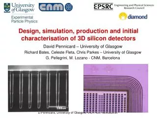
David Pennicard, University of Glasgow Simulation results from double-sided and standard 3D detectors Celeste Fleta, Chris Parkes, Richard Bates – University of Glasgow G. Pellegrini, M. Lozano - CNM, Barcelona 10th RD50 Workshop, June 2007, Vilnius, Lithuania
Overview • Simulations of different 3D detectors in ISE-TCAD • Comparison of double-sided 3D and full-3D detectors before irradiation • Radiation damage models • Preliminary results of radiation damage modelling
Overview • Simulations of different 3D detectors in ISE-TCAD • Comparison of double-sided 3D and full-3D detectors before irradiation • Radiation damage models • Preliminary results of radiation damage modelling
Double-sided 3D detectors • Proposed by CNM, also being produced by IRST • Columns etched from opposite sides of the substrate • Metal layer on back surface connects bias columns • Backside biasing • Medipix configuration (55m pitch) and 300m thickness
Double-sided 3D: Depletion behaviour • ~2V lateral depletion (same as standard 3D) • ~8V to deplete to back surface of device Doping 0V 1V 10V
Double-sided 3D: Electric field Double -sided 3D Standard 3D Similar behaviour in overlap region
Double-sided 3D: Electric field at front Low fields around front High field at column tip Electric field matches full 3D where columns overlap
Detector Column length 90% collection 99% collection Double-sided 3D 250μm 0.75ns 2.5ns Double-sided 3D 270μm 0.40ns 1.0ns Double-sided 3D 290μm 0.35ns 0.5ns Standard 3D 300μm 0.35ns 0.5ns Double-sided 3D detectors: Collection time Simulated particle track passing midway between n+ and p+ columns Variation in charge collection time with choice of device structure
Overview • Simulations of different 3D detectors in ISE-TCAD • Comparison of double-sided 3D and full-3D detectors before irradiation • Radiation damage models • Preliminary results of radiation damage modelling
Type Energy (eV) Trap σe (cm2) σh (cm2) η (cm-1) Acceptor Ec-0.42 VV 2.0*10-15 2.0*10-14 1.613 Acceptor Ec-0.46 VVV 5.0*10-15 5.0*10-14 0.9 Donor Ec+0.36 CiOi 2.5*10-14 2.5*10-15 0.9 University of Perugia trap models • 2 Acceptor levels: Close to midgap • Leakage current, negative charge (Neff), trapping of free electrons • Donor level: Further from midgap • Trapping of free holes IEEE Trans. Nucl. Sci., vol. 53, pp. 2971–2976, 2006 “Numerical Simulation of Radiation Damage Effects in p-Type and n-Type FZ Silicon Detectors”, M. Petasecca, F. Moscatelli, D. Passeri, and G. U. Pignatel Ec Perugia P-type model (FZ) - - - 0 Ev
University of Perugia trap models • Aspects of model: • Leakage current – reasonably close to α=4.0*10-17A/cm • Depletion voltage – matched to experimental results (M. Lozano et al., IEEE Trans. Nucl. Sci., vol. 52, pp. 1468–1473, 2005) • Carrier trapping – • Model reproduces CCE tests of 300m pad detectors • But trapping times don’t match experimental results Link between model and experiment • Experimental trapping times for p-type silicon (V. Cindro et al., IEEE NSS, Nov 2006) up to 1015neq/cm2 • βe= 4.0*10-7cm2s-1 βh= 4.4*10-7cm2s-1 • Calculated values from p-type trap model • βe= 1.6*10-7cm2s-1 βh= 3.5*10-8cm2s-1
Type Energy (eV) Trap σe (cm2) σh (cm2) η (cm-1) Acceptor Ec-0.42 VV 9.5*10-15 9.5*10-14 1.613 Acceptor Ec-0.46 VVV 5.0*10-15 5.0*10-14 0.9 Donor Ec+0.36 CiOi 3.23*10-13 3.23*10-14 0.9 Altering the trap models • Priorities: Trapping time and depletion behaviour • Leakage current should just be “sensible”: α = 2-10 *10-17A/cm • Chose to alter cross-sections, while keeping σh/σe constant Carrier trapping: Space charge: Modified P-type model
Type Energy (eV) Trap σe (cm2) σh (cm2) η (cm-1) Acceptor Ec-0.42 VV 9.5*10-15 9.5*10-14 1.613 Acceptor Ec-0.46 VVV 5.0*10-15 5.0*10-14 0.9 Donor Ec+0.36 CiOi 3.23*10-13 3.23*10-14 0.9 Modified P-type model and experimental data “Comparison of Radiation Hardness of P-in-N, N-in-N, and N-in-P Silicon Pad Detectors”, M. Lozano et al., IEEE Trans. Nucl. Sci., vol. 52, pp. 1468–1473, 2005 α=3.75*10-17A/cm Experimentally, α=3.99*10-17A/cm3 after 80 mins anneal at 60˚C (M. Moll thesis)
Type Energy (eV) Trap σe (cm2) σh (cm2) η (cm-1) Acceptor Ec-0.42 VV 2.0*10-15 1.2*10-14 13 Acceptor Ec-0.50 VVO 5.0*10-15 3.5*10-14 0.08 Donor Ec+0.36 CiOi 2.0*10-18 2.5*10-15 1.1 Perugia N-type model Perugia N-type model (FZ) Donor removal • Works similarly to the p-type model • Donor removal is modelled by altering the substrate doping directly • Experimental trapping times for n-type silicon (G. Kramberger et al., NIMA, vol. 481, pp297-305, 2002) • βe= 4.0*10-7cm2s-1 βh= 5.3*10-7cm2s-1 • Calculated values from n-type trap model • βe= 5.3*10-7cm2s-1 βh= 4.5*10-8cm2s-1 KC=(2.2±0.2)*10-2cm-1
Type Energy (eV) Trap σe (cm2) σh (cm2) η (cm-1) Acceptor Ec-0.42 VV 1.5*10-15 0.9*10-14 13 Acceptor Ec-0.5 VVO 5.0*10-15 3.5*10-14 0.08 Donor Ec+0.36 CiOi 2.5*10-17 3.1*10-15 1.1 Modified N-type model “Characterization of n and p-type diodes processed on Fz and MCz silicon after irradiation with 24 GeV/c and 26 MeV protons and with reactor neutrons”, Donato Creanza et al., 6th RD50 Helsinki June 2-4 2005 α=2.35*10-17A/cm Experimentally, α=3.99*10-17A/cmafter 80 mins anneal at 60˚C (M. Moll thesis)
Bug in ISE-TCAD version 7 • Currently using Dessis, in ISE-TCAD v7 (2001) • Non time-dependent simulations with trapping are OK • Error occurs in transient simulations with traps • Carrier behaviour in depletion region is OK • Displacement current is miscalculated • This affects currents at the electrodes • This bug is not present in the latest release of Synopsis TCAD (2007) • Synopsis bought ISE TCAD, and renamed Dessis as “Sentaurus Device” • Don’t know which specific release fixed the problem Correct behaviour: Error:
Test of charge trapping in Synopsis TCAD • Simulated a simple diode with carriers generated at its midpoint No traps “Double step” seen because electrons are collected before holes
Test of charge trapping in Synopsis TCAD • Simulated a simple diode with carriers generated at its midpoint • Acceptor and donor traps further from the midgap • Produces charge trapping but little change in Neff • Trap levels should give τe≈ τh ≈ 1ns ISE TCAD traps ?!
Test of charge trapping in Synopsis TCAD • Simulated a simple diode with carriers generated at its midpoint • Acceptor and donor traps further from the midgap • Produces charge trapping but little change in Neff • Trap levels should give τe≈ τh ≈ 1ns Synopsis traps With traps, signal decays as exp (-t/1ns) as expected
Overview • Simulations of different 3D detectors in ISE-TCAD • Comparison of double-sided 3D and full-3D detectors before irradiation • Radiation damage models • Preliminary results of radiation damage modelling
Full 3D – Depletion voltage (p-type) • Depletion voltage is low, but strongly dependent on pitch • Double sided 3D shows the same lateral depletion voltage as full 3D 133m 50m 55m
Full 3D – electric field at 100V Full depletion is achieved well under 100V, but electric field is altered No damage 1016 neq/cm2
Double-sided 3D – front surface Once again, double-sided devices show different behaviour at front and back surfaces No damage 1016 neq/cm2
Double-sided 3D – back surface Region at back surface depletes more slowly – not fully depleted at 100V bias No damage 1016 neq/cm2 Undepleted
3 133m 8 50m 50m Further work • Simulate charge collection! • Consider effects of different available pixel layouts • CCE, depletion voltage, insensitive area, capacitance
Conclusions • Double-sided 3D detectors: • Behaviour mostly similar to standard 3D • Depletion to back surface requires a higher bias • Front and back surfaces show slower charge collection • Radiation damage model • Trap behaviour is directly simulated in ISE-TCAD • Trap models based on Perugia models, altered to match experimental trapping times • Preliminary tests of damage model with 3D • Relatively low depletion voltages, but electric field pattern is altered • Double-sided 3D shows undepleted region at back surface at high fluences
3D detectors • N+ and p+ columns pass through substrate • Fast charge collection • Low depletion voltage • Low charge sharing • Additional processing (DRIE for hole etching) Planar 3D
Breakdown in double-sided 3D • Breakdown occurs at column tips around 230V • Dependent on shape, e.g. 185V for square columns
Breakdown in double-sided 3D • With 1012cm-2 charge, breakdown at 210V Front Back P-stop Column tips P+ base
Example of ISE TCAD bug P+ In simulation, charge deposited at the front N+ 300μm
Example of ISE TCAD bug P+ N+ Holes drift 300μm
Full 3D – Depletion voltage (p-type) • Depletion voltage is low, but strongly dependent on pitch • Double sided 3D shows the same lateral depletion voltage as full 3D 133m 50m 55m
Weighting fields and electrode layouts Symmetrical layout of n+ and p+ Weighting potential is the same for electrons and holes Electric field, 100V bias Weighting potential
Weighting fields and electrode layouts 3 bias columns per readout column Weighing potential favours electron collection Electric field, 100V bias Weighting potential
Future work – Design choices with 3D • Choice of electrode layout: • In general, two main layouts possible • Second option doubles number of columns • However, increasing no. of p+ columns means larger electron signal
133m 50m Future work – Design choices with 3D • ATLAS pixel (400m * 50m) allows a variety of layouts • No of n+ electrodes per pixel could vary from ~3-8 • Have to consider Vdep, speed, total column area, capacitance • FP420 / ATLAS run at Stanford already has different layouts • CMS (100 m * 150m) 3 50m 8