Download
1 / 2
30 likes | 257 Vues
Grain Boundary Loops in Graphene Phillip N. First, Georgia Tech Research Corporation, DMR 1106131.

E N D
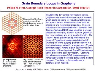
Grain Boundary Loops in Graphene Phillip N. First, Georgia Tech Research Corporation, DMR 1106131 In addition to its vaunted electrical properties, graphene has extraordinary mechanical strength, which could be useful for robust nanostructures. But atomic defects would detract from both its electronic and mechanical properties. In recent theoretical and experimental work, scientists from Georgia Tech and NIST have identified a unique defect that could play a role in both the growth of this novel material and in its tensile strength. The “flower” defect pictured at top left consists of a group of 7 graphene hexagons rotated by 30o with respect to the outlying graphene lattice. It is the lowest energy defect in a larger class of “grain boundary loops,” where a grain boundary can be associated with each pair of 5- and 7-carbon rings (blue, pink) in the boundary region. Scanning tunneling microscopy (STM) images compare remarkably well to theoretical calculations (bottom images). The defect is fortunately rare in carefully-grown material. Schematic of the flower grain boundary loop. Shaded regions show 5- and 7-carbon rings. (b) Theory. Calculated local density of states (DFT) with overlay of atom positions. (a) Experiment. STM image of a flower defect in graphene. Supported in part by NSF DMR-1106131, DMR-0804908 and DMR-0820382 (MRSEC)
Research Experience for High School Teachers Phillip N. First, Georgia Tech Research Corporation, DMR 1106131 Clean and sharp tips (needles) are essential for acquiring atomic-resolution images using scanning tunneling microscopy (STM). During Summer 2011, High School teacher Brian Heglund learned electrochemical etching techniques for the preparation of STM tips. He then set up a new etching apparatus under an optical microscope (including computer image acquisition), experimented with different etching parameters, and measured tip sharpness using a scanning electron microscope (SEM), which has much better resolution than an optical microscope. The etching station is shown at top-left and SEM images of 3 tips etched with etch potential (top) too low, (center) optimal, and (bottom) too high. Brian used these and other SEM images to tune the tip etching parameters. • SUMMER 2011: • Brian Heglund (Etowah HS, Cherokee co., GA) created a new tip-etching station and measured tip sharpness using a scanning electron microscope. Partial personnel support for the RET program comes from DMR-0820382 (MRSEC)