FULL WAVE RECTIFIER
FULL WAVE RECTIFIER. Center-Tapped Bridge. Full-Wave Rectification – circuit with center-tapped transformer. Positive cycle , D2 off, D1 conducts; Vo – Vs + V = 0 Vo = Vs - V . Negative cycle , D1 off, D2 conducts; Vo – Vs + V = 0 Vo = Vs - V .


FULL WAVE RECTIFIER
E N D
Presentation Transcript
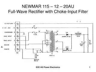
FULL WAVE RECTIFIER Center-Tapped Bridge
Full-Wave Rectification – circuit with center-tapped transformer • Positive cycle, D2 off, D1 conducts; Vo – Vs + V = 0 Vo = Vs - V • Negative cycle, D1 off, D2 conducts; Vo – Vs + V = 0 Vo = Vs - V • Since a rectified output voltage occurs during both positive and negative cycles of the input signal, this circuit is called a full-wave rectifier. • Also notice that the polarity of the output voltage for both cycles is the same
Vp -V V Vs = Vpsin t Notice again that the peak voltage of Vo is lower since Vo = Vs - V • Vs < V, diode off, open circuit, no current flow,Vo = 0V
Full-Wave Rectification –Bridge Rectifier • Positivecycle, D1 and D2 conducts, D3 and D4off; • + V + Vo + V – Vs = 0 • Vo = Vs - 2V • Negative cycle, D3 and D4 conducts, D1 and D2 off • + V + Vo + V – Vs = 0 • Vo = Vs - 2V • Also notice that the polarity of the output voltage for both cycles is the same
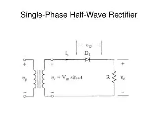
A full-wave center-tapped rectifier circuit is shown in Fig. 3.1. Assume that for each diode, the cut-in voltage, V = 0.6V and the diode forward resistance, rf is 15.The load resistor, R = 95 . Determine: • peak output voltage, Vo across the load, R • Sketch the output voltage, Vo and label its peak value. ( sine wave )
SOLUTION • peak output voltage, Vo Vs(peak) = 125 / 25 = 5V V +ID(15) + ID (95) - Vs(peak) = 0 ID= (5 – 0.6) / 110 = 0.04 A Vo (peak) = 95 x 0.04 = 3.8V Vo 3.8V t
Duty Cycle: The fraction of the wave cycle over which the diode is conducting.
EXAMPLE 3.1 – Half Wave Rectifier Determine the currents and voltages of the half-wave rectifier circuit. Consider the half-wave rectifier circuit shown in Figure. Assume and . Also assume that Determine the peak diode current, maximum reverse-bias diode voltage, the fraction of the wave cycle over which the diode is conducting. -VR + VB + 18.6 = 0 VR = 24.6 V - VR + A simple half-wave battery charger circuit - +
The peak inverse voltage (PIV) of the diode is the peak value of the voltage that a diode can withstand when it is reversed biased
Example: Half Wave Rectifier Given a half wave rectifier with input primary voltage, Vp = 80 sin t and the transformer turns ratio, N1/N2 = 6. If the diode is ideal diode, (V = 0V), determine the value of the peak inverse voltage. • Get the input of the secondary voltage: • 80 / 6 = 13.33 V • PIV for half-wave = Peak value of the input voltage = 13.33 V
EXAMPLE 3.2 • Calculate the transformer turns ratio and the PIV voltages for each type of the full wave rectifier • center-tapped • bridge • Assume the input voltage of the transformer is 220 V (rms), 50 Hz from ac main line source. The desired peak output voltage is 9 volt; also assume diodes cut-in voltage = 0.6 V.
Solution: For the centre-tapped transformer circuit the peak voltage of the transformer secondary is required The peak output voltage = 9V Output voltage, Vo = Vs - V Hence, Vs = 9 + 0.6 = 9.6V Peak value = Vrms x 2 So, Vs (rms) = 9.6 / 2 = 6.79 V The turns ratio of the primary to each secondary winding is The PIV of each diode: 2Vs(peak) - V = 2(9.6) - 0.6 = 19.6 - 0.6 = 18.6 V
Solution: For the bridge transformer circuit the peak voltage of the transformer secondary is required The peak output voltage = 9V Output voltage, Vo = Vs - 2V Hence, Vs = 9 + 1.2 = 10.2 V Peak value = Vrms x 2 So, Vs (rms) = 10.2 / 2 = 7.21 V The turns ratio of the primary to each secondary winding is The PIV of each diode: Vs(peak)- V = 10.2 - 0.6 = 9.6 V