Download
1 / 14
140 likes | 241 Vues
Learn layout recommendations, power supply considerations, and EMC factors to optimize your PCB design for DVI applications. Ensure signal integrity, reduce EMI, and enhance performance with expert insights.

E N D
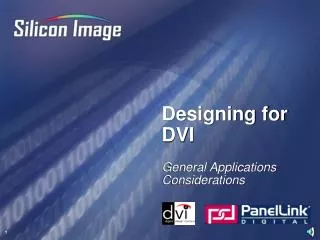
Designing for DVI General Applications Considerations
Design Issues to Consider • Layout Recommendations • Power supply considerations • EMC considerations
Layout Recommendations • Route differential pairs together • Avoid excessive or asymmetric vias
Layout Recommendations (cont’d) • Series damping resistors on data, clock, control signal inputs to TX GPU • Reduces signal ringing, noise
Signal Lines IC Cut in GND or poor HF contact IC Common-Mode Current Layout Recommendations (cont’d) • Four layer PCB • Solid ground plane Signal GND
Low Emissions Signal Signal Return Current Trace Return Current GND Plane Layout Considerations (cont’d) High Emissions GND Plane
Power Supply Considerations • Voltage regulator on TX PVCC supply Switch-mode Power Supply PVCC, PVCC2 +5V +3.3V Switching Noise ~45-60KHz • Switching noise can cause PLL jitter • VREG greatly reduces supply noise
EMC Considerations • Even though PanelLink operates at over 1GHz, most emissions are still caused by parallel data • Some high frequency emissions near 1GHz are possible, but are related to mechanical contact
EMC Considerations: Data Lines • Damping resistors, short data path Minimize Length
Good contact between Shield and connector Shell Broad contact Between connector And Bracket Solid contact between Bracket and chassis EMC Considerations: Ground Contact • Good, broad contact between connector shells and the I/O bracket • Broad contact between the I/O bracket and the system chassis • Good 360o contact between connector shell and cable shield • Good contact between motherboard GND and chassis • Helps with high frequency emissions
Signal GND/RTN Cable Shield Display Chassis EMC Considerations: Ground Contact • The chassis is the common GND reference • Do not have floating grounds PCB GND 2 PCB GND 2 Monitor PCB GND PCB GND 1 Shielding Host Chassis Shielding
Ground Contact: Example PCB 2 Signal & GND (Return) Cable Shield PCB 1 PCB 3 Main Chassis Remote Chassis ° 360 Clamps or Connector Shells Shielding Shielding
Summary • Voltage regulator strongly recommended on TX PVCC • Damping resistors on all parallel data lines • Improves signal integrity and EMI • Solid ground plane • Use chassis as common GND reference
Conclusion • PanelLink is very robust, but is still a high-speed gigabit serial link • Higher data rate than gigabit ethernet • Reference schematics provided • Silicon Image is the leader in experience and knowledge of this technology • Applications knowledge • Local and factory support • Production and testing