Download
1 / 1
10 likes | 163 Vues
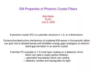
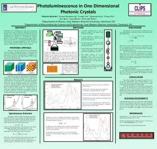
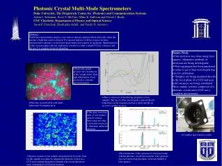
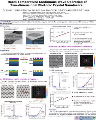
Room Temperature Continuous-wave Operation of Two-dimensional Photonic Crystal Nanolasers. d. d. a. r. E-beam lithography. PMMA. PMMA. 300nm. SiNx. SiNx. InGaAsP. InGaAsP. 200nm. Sapphire. Sapphire. 500 nm. RIE. ICP. SiNx. InGaAsP. InGaAsP. Sapphire. Sapphire. 500 nm.

E N D
Room Temperature Continuous-wave Operation of Two-dimensional Photonic Crystal Nanolasers d d a r E-beam lithography PMMA PMMA 300nm SiNx SiNx InGaAsP InGaAsP 200nm Sapphire Sapphire 500 nm RIE ICP SiNx InGaAsP InGaAsP Sapphire Sapphire 500 nm ~580 nm Yu-Chen Liu1,2 (劉育辰), Yi-Chun Yang1(楊怡君), Zi-Chang Chang2(張子倉), M. C. Wu2(吳孟奇) and M. H. Shih1,3 (施閔雄) 1Research Center for Applied Science (RCAS), Academia Sinica, Taiwan. 2Department of Electrical Engineering, National Tsing Hua University , Taiwan. 3Department of Photonics, National Chiao Tung University, Taiwan. Address: 128 Sec.2, Academia Rd., Nankang, Taipei 11529, Taiwan Phone : 03-5712121 ext.59470, Fax : 03-5745233, Email : mhshih@gate.sinica.edu.tw Abstract: Photonic crystal nanolasers had been fabricated on a sapphire substrate. The room temperature continuous-wave (CW) lasing near 1550 nm had been achieved. Motivation Lasing wavelength vs lattice constant • Nanocavity with about 580 nm in diameter • High side-mode suppression-ratio , which is over 20 dB • Low threshold 0.85 mW, but after estimating the material absorption, surface reflectivity of the cavity structure, the effective threshold power The structure can only lase under pulsed condition. The structure can lase underCW condition. is only 35 μW Thermal conductivity Air : 2.5×10⁻⁵ W/cm‧K Thermal conductivity Sapphire : 5×10⁻¹ W/cm‧K Point-shift CW photonic crystal nanolaser on sapphire Point-shift here means shifts of two lattice points to form the defect cavity, like ( a ). Fabrication This is the smallest photonic crystal cavity on the substrate so far. In the fabrication, first the InGaAsP wafer are bonded with the sapphire wafer , the following process are showed in the following flow charts : SEM image (Top view) SEM image (angle view) FDTD simulated mode profile a = lattice constant r = radius d = shifts of lattice points mode volume 0.014μm3 ~1.15(λ/2n)3 Lasing spectrum (CW) under room temperature Light-in light-out curve (LL-curve) D1 CW photonic crystal nanolaser on sapphire D1 here means one hole was removed from the hexagon photonic crystal lattices to form a defect cavity. SEM image (Top view) SEM image (angle view) FDTD simulated mode profile Lasing wavelength vs lattice constant • SmallestCW laser on the substrate • Ultrasmall mode volume, only 0.014μm3 • The effective threshold power is only 40 μW after estimating the material absorption, surface reflectivity of the mode volume 0.023μm3 ~1.5(λ/2n)3 Lasing spectrum (CW) under room temperature Light-in light-out curve (LL-curve) cavity structure Summary We have demonstrated the D1 and point-shift sapphire-bonded photonic crystal nanolasers under CW operating conditions at room temperature. The CW nanolasers has ultrasmall size, excellent heat dissipation and low threshold. It is very useful for future dense integrated photonic circuits.