ISE
ISE . ISE software tools. ISE is Xilinx software design tools that concentrate on delivering you the most productivity available for your Spartan-IIE™ logic performance. With The ProActive Timing Closure technology


ISE
E N D
Presentation Transcript
ISE software tools • ISE is Xilinx software design tools that concentrate on delivering you the most productivity available for your Spartan-IIE™ logic performance. • With The ProActive Timing Closure technology you get the fastest runtimes in programmable logic ensuring you reach your performance goals quicker. • The Incremental Design delivers faster re-compile times with guaranteed performance. • Optional ChipScope Pro verification tools whisk you through real-time debugging. Tatjana Petrovic 249/98
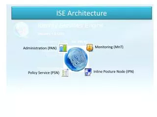
The widest variety of design entry support • ISE offers powerful Schematic Entry capabilities integrated in the Project Navigator • ISE projects can include schematics as well as HDL source to define a design (HDL editor). • After the source file is created, the Project Navigator invokes the Engineering Capture System (ECS) tool to enable creation and modification of the schematic design. • The three principle components of ECS are: the Schematic Editor, the Symbol Editor, and HDL netlisters. Tatjana Petrovic 249/98
The widest variety of design entry support • The Schematic Editor is the main schematic-creation interface. • The Symbol Editor allows creation and modification of symbols that are used in the Schematic Editor. • The netlist program translates a schematic into an HDL model that is used for synthesis and simulation of the design. Tatjana Petrovic 249/98
Timing-Driven Place and Route for programmable logic In ISE when you specify timing requirements for critical paths, performance is dramatically improved through tools such as • Timing Analyzer, • Constraints Editor with TimeSpecs™ FPGA Editor and • Floorplanner. Now, ProActive™ Timing Closure provides the most advanced technology to help your designs meet timing specifications much more quickly than traditional methods. Tatjana Petrovic 249/98
Types of Devices: FPGA and CPLD • The CPLD (complex logic device) has a PAL-like architecture and is non-volatile. It gives relatively good performance (up to 250 MHz) and is well suited for combinational logic circuits and control logic of medium complexity (up to about 10,000 logic gates). • The FPGA (field programmable gate array )device has an array-like architecture and is volatile (SRAM based). It makes use of lookup tables (stored in the SRAM memory) to implement logic functions. Tatjana Petrovic 249/98
Design Flow Overview for CPLDs or FPGAs Tatjana Petrovic 249/98
Designs can be entered in two basic modes: Schematic HDL The schematic flow mode allows you to create a design that consists of either a top-level schematic or top-level ABEL file. It can contain underlying schematic diagrams, state machine macros, instantiated HDL (ABEL, VHDL or Verilog) macros, LogiBLOX, CORE Generator modules. The implementation tools fit the entered design into the target device architecture. Design verification includes functional simulation, in-circuit testing, and timing simulation. Functional simulation can be done after the design entry to verify the proper operation of the circuit. Timing information, such as delays, race condition, set-up and hold-time violations, is obtained from the static timing simulator and is done after the design has been compiled for the target device. Design Flow Overview Tatjana Petrovic 249/98
Project Manager • The Project Manager gives you access to all the tools that are needed to design, simulate and implement a project. • From the Manager you can also create a new project, open an existing project or delete projects. • When you create a new project e.g. MyProj, the Foundation tools will create the following files: the Project Description File (myproj.pdf), and three library files, the project libraryfile (myproj), the simulation library file (simprims) and the device library (xc4000x) files. Tatjana Petrovic 249/98
Schematic Entry Tatjana Petrovic 249/98
Schematic Entry Tatjana Petrovic 249/98
The Alternative Design Entry • An alternative way to use the Schematic editor to enter a design is by using a behavioral-like description. • TheXilinx Foundation F2.1 tools allow you to enter a design using ABEL, VHDL or Verilog. • An ABEL-based design will be entered using the Schematic flow mode, while a VHDL/Verilog-based design needs to be entered using the HDL-flow mode. Tatjana Petrovic 249/98
Design Implementation • The implementation tools will translate the netlist (schematic, HDL), place and route (or fit for CPLDs) the design in the target device and generate a bitstream that can be downloaded into the device. • The implementation is typically done, after the design has been verified by the functional simulator. • Implemenation needs to be done prior to doing a timing simulation, since timing information depends on a specific target device and the way the design has been placed and routed on the device Tatjana Petrovic 249/98
Implementation • The first step is the translation of the design file (EDIF file) in a proper format (NGD file - Native Generic Database). • The next step is mapping of the design to the specific target device. The mapper optimizes the logic, trims or removes logic and maps the design in the targeted FPGA device. • Next is the Place&Route operation, followed by the generation of the timing information for use by the timing simulator. • The final step is the generation of the Bitstream which is a configuration file that can be used to program the FPGA. Tatjana Petrovic 249/98
Implementation Report Files • Pad reports: the assignments of the I/O pins, the same as specified on the schematic. • Map report: if logic has been removed (as part of the optimization) or added. • The Place&Route report indicates how much of the device has been utilized. It gives also a rough estimate of the average interconnection delay. Tatjana Petrovic 249/98
Constraint Files • There are two types of constraints: (1) location and (2) timing. • Location constraints allow you to control mapping and positioning of logic elements in the target device, such as the location of the pads (I/O pins). • Timing constraints inform the system which paths are critical and need short interconnections (high speed lines) in order to ensure that your design's performance functions properly under worst-case conditions. • Constraints can be entered by placing constraints on the schematic or in the ABEL file, or using the Constraint Editor. Tatjana Petrovic 249/98
Simulating a circuit • Design verification is an important aspect of each project design. • For complex designs which consists of multiple modules (macros) it is recommended that you simulate each module separately before simulating the overall project. • Design verification consists of functional simulation and timing simulation. • Functional simulation can be done after the schematic has been entered or a HDL file has been created and synthesized. Functional simulation gives information about the logic operation of the circuit. It does not provide any information about timing delays. • Timing simulation will tell you how fast signals travel through the gates and how fast the overall circuit can be operated. Timing information can only be obtained after the design has been implemented Tatjana Petrovic 249/98
Functional Simulation Logic Simulator window (Screen clip from Xilinx (TM) Foundation software) Tatjana Petrovic 249/98
Functional Simulation Component Selection windows (Screen clip from Xilinx (TM) Foundation software) Tatjana Petrovic 249/98
Timing Simulation Timing simulation, showing the delay of the output signal (Buzzer) in relation to the input signal (Screen clip from Xilinx (TM) Foundation software) Tatjana Petrovic 249/98
Looking at the Floor Plan: the FPGA Editor • You can use the FPGA Editor to look how the device's resources have been used and placed on the FPGA. • You can also use this application to place and route critical components before running the automatic place and route tools on your design. • The Editor allows you to display different levels of details on the FPGA such as short wires, long wires, switch boxes, routing between components, components, etc. Tatjana Petrovic 249/98
The FPGA Editor Figure shows the FPGA editor window with a view of the FPGA floorplan, around the area where the logic circuit has been placed. The three blue boxes are the I/O blocks, and the red one is the logic block. The switching network and the routing of the signals to the logic block are shown as well. Tatjana Petrovic 249/98