Download
1 / 12
140 likes | 285 Vues
Design and Simulation of Multiplexer Cell Resistant to Side Channel Attacks. Authors : Milena Stanojlović , milena @ venus.elfak.ni.ac.rs Predrag Petković , predrag . petkovic @ elfak.ni.ac.rs. Content. Introduction NSDDL method MUX2x1 NSDDL cell Conclusion. Introduction.

E N D
Design and Simulation of Multiplexer Cell Resistant to Side Channel Attacks Authors: Milena Stanojlović, milena@venus.elfak.ni.ac.rs Predrag Petković, predrag.petkovic@elfak.ni.ac.rs
Content • Introduction • NSDDL method • MUX2x1 NSDDL cell • Conclusion
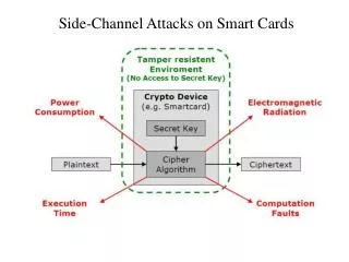
Introduction Data protection is very important in everyday life and for that reason cryptography received a significant position. Important information, such as secret keys, can be obtained by observing the power consumption, the electromagnetic radiation, the timing information etc. Common to all these methods is analysis of information that leaks from physically implemented hardware.
NSDDL method Cells resistant to SCA (Side Channel Attacks) are based on the idea that each combination of input signals results in the same power consumption. This is possible when every logic cell has the counterpart that will react complementary. Therefore every cell has two outputs denoted as true and false. The hardware is doubled, but the effect of masking the true function of the cell is gained.
NSDDL method NSDDL method is based on the three phase clocking. This is achieved by using a dynamic NOR circuit (DNOR). It is the integral part of the control logic and NSDDL cells. The first phase named pre-charge is aimed to drive all outputs (true and false) of all logic cells go to high logic level. In the second phase, known as evaluation phase true outputs takes desired value and false output takes the complementary value. The third phase is named discharge because all outputs go to the low logic level. Fig. 1. DNOR circuit Fig. 2. Time waveforms of control signals for DNOR cell
MUX2x1 NSDDL cell Block diagram of MUX2x1 NSDDL cell is presented in figure 3. Observing this figure one can see that these blocks have the same structure. It consists of two DNOR cells and one MUX2x1. The number of input and output signals in these blocks is the same but input signals are sorted differently. In the False block, inputs A and B exchange their positions because true and false output signals in evaluation phase must be complementary. That is seen in Table I. Fig.3 Block scheme of MUX2x1 NSDDL cell Table I Truth table for NSDDL MUX2x1 cell
Waveforms in figure 4 present in top down direction: excitation voltages A and B (1st and 2nd), Discharge and Pre-charge control signals (3rd and 4th), selection signal (5th), IDD and output voltage of NSDDL cell (6th and 7th), and IDD and output voltage for standard MUX2x1 cell (8th and 9th). Comparing IDD waveforms for NSDDL and standard cell, for the same input signals, one can see very clear difference. Supply current of MUX2x1 NSDDL has regular pattern independent on output logic states, contrary than a supply current of standard cell. Fig. 4 Waveforms of characteristic signals in NSDDL and standard MUX2x1 cell
To quantify resistivity to SCA we have adopted a measure based on computed integral of consumed power in time (energy) according to (1). (1) Energy consumption is observed during one cycle of input signal change. For MUX2x1 NSDDL this cycle lasts for all three operational phases. In order to get better insight into behavior of both cells we derived the following parameters from the simulation results: - maximum energy (Emax), - minimum energy (Emin) - average energy (Eav) - relative difference in respect to Eav - standard deviation - Normalized Standard Deviation (NSD) in respect to Eav
Table II Characteristics comparison of standard and NSDDL MUX2x1 cell As a measure of SCA resistance we considered normalized standard deviation. The total improvement of the resistivity to SCA in comparison with standard multiplexer cell is about 60 times in favor to MUX2x1 NSDDL cell.
Figure 6 shows profile of energy consumption during ten cycles of input signal change for both cells. Standard MUX2x1 cell characterize lower average energy and considerable dispersion of values corresponding to particular input signal combinations. Oppositely, the energy profile of MUX2x1 NSDDL cell shows no deviation and is very uniform. Fig.6 Energy consumption during ten cycles of input signal change for both cells Fig.5 Layout of SCA resistant MUX2x1 cell
Conclusion This paper presents simulation results that prove resistance of MUX2x1 cell designed by NSDDL method to side channel attack. The resistance to SCA was monitored through energies required for output transition under different combination of input signal. The cell is resistive if all changes require the same energy. As a measure for a cell resistance to SCA we considered standard deviation normalized to the average energy (NSD). NSDDL cell has NSD nearly 1%. This is 60 times less with regard to standard cell. This is sufficient to conclude that MUX2x1 NSDDL cell is immune to SCA.