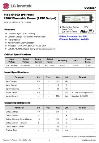
Stk 6031 8-Bit Microcontroller Features and Functions
Stk 6031 is an 8-bit microcontroller with 64KB flash memory, multiple CPU clock options, full-duplex UART, and 5 I/O ports. It supports interrupts, power-saving modes, and has on-chip RAM and special function registers.

Stk 6031 8-Bit Microcontroller Features and Functions
E N D
Presentation Transcript
Features • 8-bit microcontroller (8051 CPU) - stantadard 80c51 instruction set - Option for multiple CPU clock(XTAL1, XTAL1x2, XTAL1/3). - Normal mode, idle mode and stop mode. • Program Memory: 64 Kbytes on-chip flash memory - with hardware ISP (in-system programming) - program code protection • Main Data RAM 256 Bytes(upper128+lower128) of on-chip SRAM • Aux Memory (AUX RAM): 768 bytes of SRAM • SFRs: 47
Timers: Timer0, Timer1 and Timer2 • On-chip watchdog timer • Full-duplex UART • Five I/O Ports: Port0, Port1, Port2, Port3, Port4(P4.0~4P.3) • Interuppts: 6 Sources,2 Priority level,6 vectored addresses • 4 chanel, 6-bit ADC • 5 channel,8-bit PWM • CPU operating frequency: 2 to 30 MHz • Operating voltage Range: 2.7 to 3.6 volts • Reliability of 64 kB flash memory: data retention 10 years at room temp, no of read/write cycle>20k
Central Processing Unit • Instruction set and addressing mode are compatible with 8051 microcontroller. 1-CPU Clock & Chip Configuration Register: • Stk 6031 can be configured to run at different frequencies by use of bit2 and bit1 of CHIPCON.
Instuction Cycle • CPU timing for single cycle instuction Program Staus Word Register;
MemoryOrganization • It has 4 blocks 0f on-chip memories, these are: - 65536 bytes of flash program memory - 256 of main data RAM - 768 bytes of Aux memory, and - 47 bytes of special function registors
Auxiliary Memory • It has 64 Kbytes of auxiliary memory wnich can be accessed by MOVX instruction. • Physically it is devided into two blocks: - On-chip block: 768 bytes, 0-767 - Off-chip block 768-65535 • MOVX@Ri, i=0,1, this instruction can access lowest 256 bytes of AUX RAM. • MOVX@DPTR can access the whole AUX memory range.
Interrupts • It supports 6 interrupt sources,2 level,6-vectored address interuupt systems. • Each interrupt can be enabled or disabled and can be assigned low or high priority level. • When interrupt occur its corresponding flag becomes high and it can be cleared by the user ISR.
Overall Interrupt System • Interrupt Enable Register:
Power Savings Modes: • It has two power savings modes : • SFR PCON controls its entry into idle mode and stop mode through bit 0 and bit 1. • Idle Mode: • It permits the interrupts,serial ports and timer to function while the CPU is halted. • When MC is in idle mode: - CPU (halted) - Timer0,Timer1,Timer2 and Watchdog timer,UART, External/internal interrupts are active. • Stop Mode: • In this mode crystal oscillator stops,SFRs and contents of on-chip RAM are preserved.Stop mode cann’t be entered when the watchdog timer is enabled. • Stop mode can be altered by external Reset.