Download

1 / 46
460 likes | 643 Vues
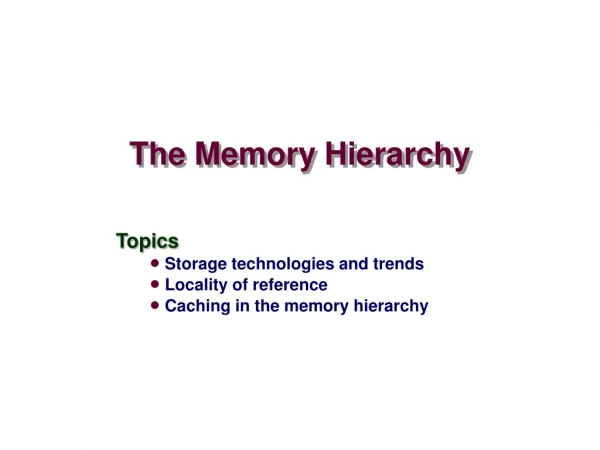
The Memory Hierarchy. Today. Storage technologies and trends Let it wash over you Locality of reference Caching in the memory hierarchy. Main Memory = DRAM. Random-Access Memory (RAM). Key features RAM is traditionally packaged as a chip.

E N D
Today • Storage technologies and trends • Let it wash over you • Locality of reference • Caching in the memory hierarchy
Random-Access Memory (RAM) • Key features • RAM is traditionally packaged as a chip. • Basic storage unit is normally a cell (one bit per cell). • Multiple RAM chips form a memory. • Static RAM (SRAM) • Each cell stores a bit with a four or six-transistor circuit. • Retains value indefinitely, as long as it is kept powered. • Relatively insensitive to electrical noise (EMI), radiation, etc. • Faster and more expensive than DRAM. • Dynamic RAM (DRAM) • Each cell stores bit with a capacitor. One transistor is used for access • Value must be refreshed every 10-100 ms. • More sensitive to disturbances (EMI, radiation,…) than SRAM. • Slower and cheaper than SRAM.
SRAM vs DRAM Summary Trans. Access Needs Needs per bit time refresh? EDC? Cost Applications SRAM 4 or 6 1X No Maybe 100x Cache memories DRAM 1 10X Yes Yes 1X Main memories, frame buffers
Lecture 14 Typical CPU clock rate 1 GHz (1ns cycle time) Typical DRAM access time 30ns (about 30 cycles) Typical main memory access 100ns (100 cycles) DRAM (30), precharge (10), chip crossings (30), overhead (30). Our pipeline designs assume 1 cycle access (1ns) Average instruction references 1 instruction word 0.3 data words This problem gets worse CPUs get faster Memories get bigger Memory delay is mostly communication time reading/writing a bit is fast it takes time to select the right bit route the data to/from the bit Big memories are slow Small memories can be made fast The Memory Bottleneck
Enhanced DRAMs • Basic DRAM cell has not changed since its invention in 1966. • Commercialized by Intel in 1970. • DRAM cores with better interface logic and faster I/O : • Synchronous DRAM (SDRAM) • Uses a conventional clock signal instead of asynchronous control • Allows reuse of the row addresses (e.g., RAS, CAS, CAS, CAS) • Double data-rate synchronous DRAM (DDR SDRAM) • Double edge clocking sends two bits per cycle per pin • Each generation incompatible (DDR, DDR2, DDR3, soon DDR4) • Nearly doubles data rate (by increasing internal clock rate) • Reduces power • By 2012, DDR3 standard for most server and desktop systems • Intel Core i7 supports only DDR3 SDRAM
Lecture 17 Better Memory System Performance • Bandwidth vs. Latency • Bandwidth = #bits transferred per cycle • Latency = time to access DRAM • Bandwidth • Memory bus width (16, 32, 64) • Multiple memory banks • Address interleaving • Multiple memory controllers (independent) • Latency • Synchronous DRAM access modes • Faster interface (Rambus)
Nonvolatile Memories • DRAM and SRAM are volatile memories • Lose information if powered off. • Nonvolatile memories retain value even if powered off • Read-only memory (ROM): programmed during production • Programmable ROM (PROM): can be programmed once • Eraseable PROM (EPROM): can be bulk erased (UV, X-Ray) • Electrically eraseable PROM (EEPROM): electronic erase capability • Flash memory: EEPROMs with partial (sector) erase capability • Wears out after about 100,000 erasings. • Uses for Nonvolatile Memories • Firmware programs stored in a ROM (BIOS, controllers for disks, network cards, graphics accelerators, security subsystems,…) • Solid state disks (replace rotating disks in thumb drives, smart phones, mp3 players, tablets, laptops,…) • Disk caches
Traditional Bus Structure Connecting CPU and Memory • A bus is a collection of parallel wires that carry address, data, and control signals. • Buses are typically shared by multiple devices. CPU chip Register file ALU System bus Memory bus Main memory Bus interface I/O bridge
Memory Read Transaction (1) • CPU places address A on the memory bus. Register file Load operation:movl A, %eax ALU %eax Main memory 0 I/O bridge A Bus interface A x
Memory Read Transaction (2) • Main memory reads A from the memory bus, retrieves word x, and places it on the bus. Register file Load operation:movl A, %eax ALU %eax Main memory 0 I/O bridge x Bus interface A x
Memory Read Transaction (3) • CPU read word x from the bus and copies it into register %eax. Register file Load operation:movl A, %eax ALU %eax x Main memory 0 I/O bridge Bus interface A x
Memory Write Transaction (1) • CPU places address A on bus. Main memory reads it and waits for the corresponding data word to arrive. Register file Store operation:movl %eax, A ALU %eax y Main memory 0 I/O bridge A Bus interface A
Memory Write Transaction (2) • CPU places data word y on the bus. Register file Store operation:movl %eax, A ALU %eax y Main memory 0 I/O bridge y Bus interface A
Memory Write Transaction (3) • Main memory reads data word y from the bus and stores it at address A. register file Store operation:movl %eax, A ALU %eax y main memory 0 I/O bridge bus interface A y
What’s Inside A Disk Drive? Spindle Arm Platters Actuator Electronics (including a processor and memory!) SCSI connector Image courtesy of Seagate Technology
Disk Geometry • Disks consist of platters, each with two surfaces. • Each surface consists of concentric rings called tracks. • Each track consists of sectors separated by gaps. Tracks Surface Track k Gaps Spindle Sectors
I/O Bus CPU chip Register file ALU System bus Memory bus Main memory Bus interface I/O bridge I/O bus Expansion slots for other devices such as network adapters. USB controller Graphics adapter Disk controller Mouse Keyboard Monitor Disk
Reading a Disk Sector (1) CPU chip CPU initiates a disk read by writing a command, logical block number, and destination memory address to a port (address) associated with disk controller. Register file ALU Main memory Bus interface I/O bus USB controller Graphics adapter Disk controller keyboard mouse Monitor Disk
Reading a Disk Sector (2) CPU chip Disk controller reads the sector and performs a direct memory access (DMA) transfer into main memory. Register file ALU Main memory Bus interface I/O bus USB controller Graphics adapter Disk controller Mouse Keyboard Monitor Disk
Reading a Disk Sector (3) CPU chip When the DMA transfer completes, the disk controller notifies the CPU with an interrupt (i.e., asserts a special “interrupt” pin on the CPU) Register file ALU Main memory Bus interface I/O bus USB controller Graphics adapter Disk controller Mouse Keyboard Monitor Disk
Solid State Disks (SSDs) I/O bus • Pages: 512KB to 4KB, Blocks: 32 to 128 pages • Data read/written in units of pages. • Page can be written only after its block has been erased • A block wears out after 100,000 repeated writes. Requests to read and write logical disk blocks Solid State Disk (SSD) Flash translation layer Flash memory Block 0 Block B-1 … … … Page 0 Page 1 Page P-1 Page 0 Page 1 Page P-1
SSD Performance Characteristics • Why are random writes so slow? • Erasing a block is slow (around 1 ms) • Write to a page triggers a copy of all useful pages in the block • Find an used block (new block) and erase it • Write the page into the new block • Copy other pages from old block to the new block Sequential read tput 250 MB/s Sequential write tput 170 MB/s Random read tput 140 MB/s Random write tput 14 MB/s Rand read access 30 us Random write access 300 us
SSD Tradeoffs vs Rotating Disks • Advantages • No moving parts faster, less power, more rugged • Disadvantages • Have the potential to wear out • Mitigated by “wear leveling logic” in flash translation layer • E.g. Intel X25 guarantees 1 petabyte (1015 bytes) of random writes before they wear out • In 2010, about 100 times more expensive per byte • Applications • MP3 players, smart phones, laptops • Beginning to appear in desktops and servers
Storage Trends SRAM Metric 1980 1985 1990 1995 2000 2005 2010 2010:1980 $/MB 19,200 2,900 320 256 100 75 60 320 access (ns) 300 150 35 15 3 2 1.5 200 DRAM Metric 1980 1985 1990 1995 2000 2005 2010 2010:1980 $/MB 8,000 880 100 30 1 0.1 0.06 130,000 access (ns) 375 200 100 70 60 50 40 9 typical size (MB) 0.064 0.256 4 16 64 2,000 8,000 125,000 Disk Metric 1980 1985 1990 1995 2000 2005 2010 2010:1980 $/MB 500 100 8 0.30 0.01 0.005 0.0003 1,600,000 access (ms) 87 75 28 10 8 4 3 29 typical size (MB) 1 10 160 1,000 20,000 160,000 1,500,000 1,500,000
CPU Clock Rates Inflection point in computer history when designers hit the “Power Wall” 1980 1990 1995 2000 2003 2005 2010 2010:1980 CPU 8080 386 Pentium P-III P-4 Core 2 Core i7 --- Clock rate (MHz) 1 20 150 600 3300 2000 2500 2500 Cycle time (ns) 1000 50 6 1.6 0.3 0.50 0.4 2500 Cores 1 1 1 1 1 2 4 4 Effective cycle 1000 50 6 1.6 0.3 0.25 0.1 10,000 time (ns)
The CPU-Memory Gap The gap widens between DRAM, disk, and CPU speeds. Disk SSD DRAM CPU
Lecture 14 The Memory Hierarchy Latency Bandwidth Registers 1 cyc 3-10 words/cycle compiler managed < 1KB 1-3cy 1-2 words/cycle hardware managed 16KB -1MB 10-15cy 1-2 word/cycle hardware managed 1MB - 12MB 50-300cy 0.5 words/cycle OS managed 64MB - 4GB 106-107cy 0.01 words/cycle OS managed 40GB+ CPU Chip L1 Cache L2 Cache Chips DRAM Disk Mechanical Tape
Locality to the Rescue! The key to bridging this CPU-Memory gap is a fundamental property of computer programs known as locality
Today • Storage technologies and trends • Locality of reference • Caching in the memory hierarchy
Locality • Principle of Locality:Programs tend to use data and instructions with addresses near or equal to those they have used recently • Temporal locality: • Recently referenced items are likely to be referenced again in the near future • Spatial locality: • Items with nearby addresses tend to be referenced close together in time
Locality Example • Data references • Reference array elements in succession (stride-1 reference pattern). • Reference variable sum each iteration. • Instruction references • Reference instructions in sequence. • Cycle through loop repeatedly. sum = 0; for (i = 0; i < n; i++) sum += a[i]; return sum; Spatial locality Temporal locality Spatial locality Temporal locality
Qualitative Estimates of Locality • Claim: Being able to look at code and get a qualitative sense of its locality is a key skill for a professional programmer. • Question: Does this function have good locality with respect to array a? intsum_array_rows(inta[M][N]) { inti, j, sum = 0; for (i = 0; i < M; i++) for (j = 0; j < N; j++) sum += a[i][j]; return sum; }
Locality Example • Question: Does this function have good locality with respect to array a? intsum_array_cols(inta[M][N]) { inti, j, sum = 0; for (j = 0; j < N; j++) for (i = 0; i < M; i++) sum += a[i][j]; return sum; }
Locality Example • Question: Can you permute the loops so that the function scans the 3-d array a with a stride-1 reference pattern (and thus has good spatial locality)? int sum_array_3d(int a[M][N][N]) { inti, j, k, sum = 0; for (i = 0; i < M; i++) for (j = 0; j < N; j++) for (k = 0; k < N; k++) sum += a[k][i][j]; return sum; }
Memory Hierarchies • Some fundamental and enduring properties of hardware and software: • Fast storage technologies cost more per byte, have less capacity, and require more power (heat!). • The gap between CPU and main memory speed is widening. • Well-written programs tend to exhibit good locality. • These fundamental properties complement each other beautifully. • They suggest an approach for organizing memory and storage systems known as a memory hierarchy.
Today • Storage technologies and trends • Locality of reference • Caching in the memory hierarchy
An Example Memory Hierarchy L0: CPU registers hold words retrieved from L1 cache Registers L1: L1 cache (SRAM) L1 cache holds cache lines retrieved from L2 cache Smaller, faster, costlier per byte L2: L2 cache (SRAM) L2 cache holds cache lines retrieved from main memory L3: Main memory (DRAM) Larger, slower, cheaper per byte Main memory holds disk blocks retrieved from local disks Local secondary storage (local disks) L4: Local disks hold files retrieved from disks on remote network servers Remote secondary storage (tapes, distributed file systems, Web servers) L5:
Caches • Cache:A smaller, faster storage device that acts as a staging area for a subset of the data in a larger, slower device. • Fundamental idea of a memory hierarchy: • For each k, the faster, smaller device at level k serves as a cache for the larger, slower device at level k+1. • Why do memory hierarchies work? • Because of locality, programs tend to access the data at level k more often than they access the data at level k+1. • Thus, the storage at level k+1 can be slower, and thus larger and cheaper per bit. • Big Idea: The memory hierarchy creates a large pool of storage that costs as much as the cheap storage near the bottom, but that serves data to programs at the rate of the fast storage near the top.
General Cache Concepts Smaller, faster, more expensive memory caches a subset of the blocks Cache 4 8 9 14 10 3 Data is copied in block-sized transfer units 4 10 Larger, slower, cheaper memory viewed as partitioned into “blocks” Memory 0 1 2 3 4 4 5 6 7 8 9 10 10 11 12 13 14 15
General Cache Concepts: Hit Data in block b is needed Request: 14 Block b is in cache: Hit! Cache 8 9 14 3 14 Memory 0 1 2 3 4 5 6 7 8 9 10 11 12 13 14 15
General Cache Concepts: Miss Data in block b is needed Request: 12 Block b is not in cache: Miss! Cache 8 9 14 3 12 Block b is fetched from memory Request: 12 12 • Block b is stored in cache • Placement policy:determines where b goes • Replacement policy:determines which blockgets evicted (victim) Memory 0 1 2 3 4 5 6 7 8 9 10 11 12 12 13 14 15
General Caching Concepts: Types of Cache Misses • Cold (compulsory) miss • Cold misses occur because the line has never been touched. • A cache whose size equals memory takes only cold misses. • Conflict miss • Conflict misses occur when the level k cache is large enough, but multiple data objects all map to the same level k block. • Arises from limited associativityand non-optimal replacement • Misses absent in a fully-associative, optimal replacement policy cache are conflict misses. • Capacity miss • Occurs when the set of active cache blocks (working set) is larger than the cache.
Examples of Caching in the Hierarchy Cache Type What is Cached? Where is it Cached? Latency (cycles) Managed By Registers 4-8 bytes words CPU core 0 Compiler TLB Address translations On-Chip TLB 0 Hardware L1 cache 64-bytes block On-Chip L1 1 Hardware L2 cache 64-bytes block On/Off-Chip L2 10 Hardware Virtual Memory 4-KB page Main memory 100 Hardware + OS Buffer cache Parts of files Main memory 100 OS Disk cache Disk sectors Disk controller 100,000 Disk firmware Network buffer cache Parts of files Local disk 10,000,000 AFS/NFS client Browser cache Web pages Local disk 10,000,000 Web browser Web cache Web pages Remote server disks 1,000,000,000 Web proxy server
Summary • The speed gap between CPU, memory and mass storage continues to widen. • Well-written programs exhibit a property called locality. • Memory hierarchies based on caching close the gap by exploiting locality.