Download
1 / 44
440 likes | 490 Vues
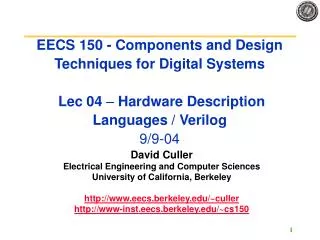
EECS 150 - Components and Design Techniques for Digital Systems Lec 09 – Counters 9-28-04. David Culler Electrical Engineering and Computer Sciences University of California, Berkeley http://www.eecs.berkeley.edu/~culler http://www-inst.eecs.berkeley.edu/~cs150. Review: Designing with FSM.

E N D
EECS 150 - Components and Design Techniques for Digital Systems Lec 09– Counters9-28-04 David Culler Electrical Engineering and Computer Sciences University of California, Berkeley http://www.eecs.berkeley.edu/~culler http://www-inst.eecs.berkeley.edu/~cs150
Review: Designing with FSM • FSMs are critical tool in your design toolbox • Adapters, Protocols, Datapath Controllers, … • They often interact with other FSMs • Important to design each well and to make them work together well. • Keep your verilog FSMs clean • Separate combinational part from state update • Good state machine design is an iterative process • State encoding • Reduction • Assignment EECS150 Fa07 Lec7 Counters
Outline • Review • Registers • Simple, important FSMs • Ring counters • Binary Counters • Universal Shift Register • Using Counters to build controllers • Different approach to FSM design EECS150 Fa07 Lec7 Counters
OUT1 OUT2 OUT3 OUT4 "0" R S R S R S R S D Q D Q D Q D Q CLK IN1 IN2 IN3 IN4 Registers • Collections of flip-flops with similar controls and logic • Stored values somehow related (e.g., form binary value) • Share clock, reset, and set lines • Similar logic at each stage • Examples • Shift registers • Counters EECS150 Fa07 Lec7 Counters
Shift-registers • Parallel load shift register: • “Parallel-to-serial converter” • Also, works as “Serial-to-parallel converter”, if Q values are connected out. • Also get used as controllers (ala “ring counters”) EECS150 Fa07 Lec7 Counters
OUT1 OUT2 OUT3 OUT4 D Q D Q D Q D Q IN CLK Shift Register module shift_reg (out4, out3, out2, out1, in, clk); output out4, out3, out2, out1; input in, clk; reg out4, out3, out2, out1; always @(posedge clk) begin out4 <= out3; out3 <= out2; out2 <= out1; out1 <= in; end endmodule What does this shift register do? What is it good for? EECS150 Fa07 Lec7 Counters
Shift Register Verilog module shift_reg (out, in, clk); output [4:1] out; input in, clk; reg [4:1] out; always @(posedge clk) begin out <= {out[3:1], in}; end endmodule EECS150 Fa07 Lec7 Counters
Shift Register Application • Parallel-to-serial conversion for serial transmission parallel outputs parallel inputs serial transmission EECS150 Fa07 Lec7 Counters
En State Next 0 Q Q 1 Q D enable Register with selective load • We often use registers to hold values for multiple clocks • Wait until needed • Used multiple times • How do we modify our D flipflop so that it holds the value till we are done with it? • A very simple FSM D Q D Q clk enable clk EECS150 Fa07 Lec7 Counters
IQ: Design Register with Set/Reset • Set forces state to 1 • Reset forces state to 0 • What might be a useful fourth option? S R S R State Next 0 0 Q Q 0 1 Q 0 1 0 Q 1 1 1 Q X D Q EECS150 Fa07 Lec7 Counters
S3 S0 S2 S1 Counters • Special sequential circuits (FSMs) that repeatedly sequence through a set of outputs. • Examples: • binary counter: 000, 001, 010, 011, 100, 101, 110, 111, 000, 001, … • gray code counter: 000, 010, 110, 100, 101, 111, 011, 001, 000, 010, 110, … • one-hot counter: 0001, 0010, 0100, 1000, 0001, 0010, … • BCD counter: 0000, 0001, 0010, …, 1001, 0000, 0001 • pseudo-random sequence generators: 10, 01, 00, 11, 10, 01, 00, ... • Moore machines with “ring” structure to STD: EECS150 Fa07 Lec7 Counters
What are they used? • Examples: • Clock divider circuits • Delays, Timing • Protocols • Counters simplify controller design… • More on this later 16MHz 64 EECS150 Fa07 Lec7 Counters
How do we design counters? • For binary counters (most common case) incrementer circuit would work: • In Verilog, a counter is specified as: x = x+1; • This does not imply an adder • An incrementer is simpler than an adder • And a counter is simpler yet. • In general, the best way to understand counter design is to think of them as FSMs, and follow general procedure. Here’s a important examples… 1 + register EECS150 Fa07 Lec7 Counters
OUT1 OUT2 OUT3 OUT4 D Q D Q D Q D Q IN CLK OUT1 OUT2 OUT3 OUT4 D Q D Q D Q D Q IN CLK Counters • Sequences through a fixed set of patterns • In this case, 1000, 0100, 0010, 0001 • If one of the patterns is its initial state (by loading or set/reset) • Mobius (or Johnson) counter • In this case, 1000, 1100, 1110, 1111, 0111, 0011, 0001, 0000 EECS150 Fa07 Lec7 Counters
“one-hot” counters0001, 0010, 0100, 1000, 0001, … “Self-starting” version: What are these good for? Ring Counters – getting started EECS150 Fa07 Lec7 Counters
Ring Counters (cont) EECS150 Fa07 Lec7 Counters
Announcements • Reading: K&B 7.1, app C. • Midterm 9/27 (week from thurs) • Regular class time. In Lab 125 Cory • Covers all material thru 9/23 • 9/23 lecture will be “putting it all together” • Review session 9/27 8-10 • See web page for additional specifics • HW 3 (current) is a good exercise (and short) • HW 4 (out thurs) will be light, then skip a week • Thurs Evening Lab is a problem! • Too many people in that section • Too many people from other sections • Lab ‘DO NOT DISTURB’ rules • You much receive checkoff in your own section (first 30 mins) • You are welcome to use the lab outside your section, but if it is during some other lab section, you much let the TA concentrate on their section. • TAs will leave promptly at 8 pm • It is your job to read lab and write Verilog before you arrive. EECS150 Fa07 Lec7 Counters
Binary Counter Design: Start with 3-bit version and generalize: a+ = a’ b+ = a b cb a 00 01 11 10 0 0 0 1 1 1 0 1 0 1 c+ = a’c + abc’ + b’c = c(a’+b’) + c’(ab) = c(ab)’ + c’(ab) = c ab c b a c+ b+ a+ 0 0 0 0 0 1 0 0 1 0 1 0 0 1 0 0 1 1 0 1 1 1 0 0 1 0 0 1 0 1 1 0 1 1 1 0 1 1 0 1 1 1 1 1 1 0 0 0 Synchronous Counters All outputs change with clock edge. EECS150 Fa07 Lec7 Counters
OUT1 OUT2 OUT3 OUT4 D Q D Q D Q D Q CLK "1" Binary Counter • Logic between registers (not just multiplexer) • XOR decides when bit should be toggled • Always for low-order bit, only when first bit is true for second bit, and so on EECS150 Fa07 Lec7 Counters
Binary Counter Verilog module counter (out4, out3, out2, out1, clk); output out4, out3, out2, out1; input in, clk; reg out4, out3, out2, out1; always @(posedge clk) begin out4 <= (out1 & out2 & out3) ^ out4; out3 <= (out1 & out2) ^ out3; out2 <= out1 ^ out2; out1 <= out1 ^ 1b’1; end endmodule EECS150 Fa07 Lec7 Counters
Binary Counter Verilog module counter (out4, out3, out2, out1, clk); output [4:1] out; input in, clk; reg [4:1] out; always @(posedge clk) out <= out + 1; endmodule EECS150 Fa07 Lec7 Counters
How do we extend to n-bits? Extrapolate c+: d+ = d abc, e+ = e abcd Has difficulty scaling (AND gate inputs grow with n) CE is “count enable”, allows external control of counting, TC is “terminal count”, is asserted on highest value, allows cascading, external sensing of occurrence of max value. TC Synchronous Counters Tb=CE*A Tc=CE*A*B Td=CE*A*B*C EECS150 Fa07 Lec7 Counters
TC Synchronous Counters • How does this one scale? • Delay grows n • Generation of TC signals very similar to generation of carry signals in adder. • “Parallel Prefix” circuit reduces delay: log2n log2n EECS150 Fa07 Lec7 Counters
ENDCBA LOAD CLK CLR RCO QDQCQBQA (2) RCO goes high (3) High order 4-bits are incremented Four-bit Binary Synchronous Up-Counter • Standard component with many applications • Positive edge-triggered FFs w/ sync load and clear inputs • Parallel load data from D, C, B, A • Enable inputs: must be asserted to enable counting • RCO: ripple-carry out used for cascading counters • high when counter is in its highest state 1111 • implemented using an AND gate (1) Low order 4-bits = 1111 EECS150 Fa07 Lec7 Counters
“Ripple” counters A3 A2 A1 A0 0000 0001 0010 0011 0100 0101 0110 0111 1000 1001 1010 1011 1100 1101 1110 1111 • Each stage is 2 of previous. • Look at output waveforms: • Often called “asynchronous” counters. • A “T” flip-flop is a “toggle” flip-flop. Flips it state on cycles when T=1. time • Discouraged • Know it exists • Don’t use it CLK A0 A1 A2 A3 EECS150 Fa07 Lec7 Counters
Up-Down Counter c b a c+ b+ a+ 0 0 0 1 1 1 0 0 1 0 0 0 0 1 0 0 0 1 0 1 1 0 1 0 1 0 0 0 1 1 1 0 1 1 0 0 1 1 0 1 0 1 1 1 1 1 1 0 Down-count Note: correct clocking EECS150 Fa07 Lec7 Counters
Extra combinational logic can be added to terminate count before max value is reached: Example: count to 12 Alternative: Odd Counts EECS150 Fa07 Lec7 Counters
Starting offset counters – use of synchronous load e.g., 0110, 0111, 1000, 1001, 1010, 1011, 1100, 1101, 1111, 0110, . . . Ending offset counter – comparator for ending value e.g., 0000, 0001, 0010, ..., 1100, 1101, 0000 Combinations of the above (start and stop value) "1" "0""1""1""0" EN DCBA LOAD CLK CLR RCO QDQCQBQA "0" "1" "0""0""0""0" EN DCBA LOAD CLK CLR RCO QDQCQBQA Offset Counters EECS150 Fa07 Lec7 Counters
output left_in right_out left_out right_in clear s0 clock s1 input Universal Shift Register • Holds 4 values • Serial or parallel inputs • Serial or parallel outputs • Permits shift left or right • Shift in new values from left or right clear sets the register contentsand output to 0s1 and s0 determine the shift function s0 s1 function 0 0 hold state 0 1 shift right 1 0 shift left 1 1 load new input EECS150 Fa07 Lec7 Counters
0 1 2 3 Design of Universal Shift Register • Consider one of the four flip-flops • New value at next clock cycle: Nth cell to N-1th cell to N+1th cell Q D CLK CLEAR clear s0 s1 new value 1 – – 0 0 0 0 output 0 0 1 output value of FF to left (shift right) 0 1 0 output value of FF to right (shift left) 0 1 1 input s0 and s1control mux Q[N-1](left) Q[N+1](right) Input[N] EECS150 Fa07 Lec7 Counters
Universal Shift Register Verilog module univ_shift (out, lo, ro, in, li, ri, s, clr, clk); output [3:0] out; output lo, ro; input [3:0] in; input [1:0] s; input li, ri, clr, clk; reg [3:0] out; assign lo = out[3]; assign ro = out[0]; always @(posedge clk or clr) begin if (clr) out <= 0; else case (s) 3: out <= in; 2: out <= {out[2:0], ri}; 1: out <= {li, out[3:1]}; 0: out <= out; endcase end endmodule EECS150 Fa07 Lec7 Counters
OUT OUT1 OUT2 OUT3 OUT4 D Q D Q D Q D Q IN CLK Pattern Recognizer • Combinational function of input samples • In this case, recognizing the pattern 1001 on the single input signal EECS150 Fa07 Lec7 Counters
Counters for Control • Big idea: to solve a big controller problem, build a very simple controller and then use it as a tool. Controller Datapath EECS150 Fa07 Lec7 Counters
bit 5 bit 0’ bit 6 bit 4 bit 3 bit 2 bit 1 ~rdy ~rdy ~rdy ~rdy ~rdy ~rdy rdy rdy rdy rdy rdy rdy Recall: Byte-bit stream with Rate Matching • How would you implement this FSM? Byte FIFO init / LD bit 0/pop ~rdy rdy ~rdy pop controller Shift register rdy LD Serial link rdy subtle bug here bit 7 / LD ~rdy EECS150 Fa07 Lec7 Counters
init / LD bit 0/pop ~rdy 0001 0010 0011 0100 0101 0110 bit 0’ 00000100 00001000 00000001 00000010 00100000 00010000 bit 0’ rdy ~rdy ~rdy ~rdy ~rdy ~rdy ~rdy ~rdy rdy rdy rdy rdy rdy rdy ~rdy rdy rdy rdy rdy rdy rdy ~rdy ~rdy Shift Reg Or Ring Counter ~rdy ~rdy ~rdy 01000000 / LD Counter for Sequencing States init / LD bit 0/pop ~rdy rdy ~rdy Binary Counter rdy ~rdy 0111 / LD ~rdy rdy EECS150 Fa07 Lec7 Counters
0011 0100 0001 0100 0001 0011 0101 0010 0110 0110 bit 0’ bit 0’ 0010 0101 ~rdy ~rdy ~rdy ~rdy ~rdy ~rdy ~rdy ~rdy ~rdy ~rdy ~rdy ~rdy rdy rdy rdy rdy rdy rdy rdy rdy rdy rdy rdy rdy CLR for “back to top” 0000/pop init / LD 0000/pop ~rdy ~rdy rdy rdy ~rdy ~rdy Binary Counter 0111 / LD, clr init 0111 / LD, clr EECS150 Fa07 Lec7 Counters
0001 0010 0011 0100 0101 0110 bit 0’ ~rdy ~rdy ~rdy ~rdy ~rdy ~rdy rdy rdy rdy rdy rdy rdy Count_Enable for Self-loop CE = rdy or (state == 0000) 0000/pop rdy ~rdy rdy ~rdy n-bit counter CE LD rdy 0111 / LD, clr init EECS150 Fa07 Lec7 Counters
Branch with LD (jump counter) X ~in in y X+1 n-bit counter CE LD ~selfloop in EECS150 Fa07 Lec7 Counters
0001 0010 0011 0100 0101 0110 1111 ~rdy ~rdy ~rdy ~rdy ~rdy ~rdy rdy rdy rdy rdy rdy rdy 4 4 4 4 Jumping 0000/pop LD = (State === 0000 & ~rdy) or (state == 1111) S = (state == 0000) rdy ~rdy rdy ~rdy 0001 0 1111 1 s LD CE 0111 / LD, clr init EECS150 Fa07 Lec7 Counters
IQ: How would you simplify this further EECS150 Fa07 Lec7 Counters
000 ~rdy rdy 0100 0101 0110 0011 1000 0010 0001 110 1101 1110 100 1111/LD,clr 101 1011 1010 1100 001 010 011 1001 ~rdy ~rdy ~rdy ~rdy ~rdy ~rdy ~rdy ~rdy ~rdy ~rdy ~rdy ~rdy ~rdy ~rdy ~rdy ~rdy ~rdy 3-bit counter rdy rdy rdy rdy rdy rdy rdy rdy rdy rdy rdy rdy rdy rdy rdy rdy rdy set CE TC init rdy LD,pop rdy/ LD, pop rdy ~rdy 111 ~rdy State Complexity vs Counter Usage ~rdy 0000/pop rdy rdy ~rdy 0111 / LD, clr EECS150 Fa07 Lec7 Counters init
Example, Bit-serial multiplier: Control Algorithm: Another Controller using Counters repeat n cycles { // outer (i) loop repeat n cycles{ // inner (j) loop shiftA, selectSum, shiftHI } shiftB, shiftHI, shiftLOW, reset } Note: The occurrence of a control signal x means x=1. The absence of x means x=0. EECS150 Fa07 Lec7 Counters
State Transition Diagram: Assume presence of two binary counters. An “i” counter for the outer loop and “j” counter for inner loop. Counter provides subsidiary state TC is asserted when the counter reaches it maximum count value. CE is “clock enable”. The counter increments its value on the rising edge of the clock if CE is asserted. EECS150 Fa07 Lec7 Counters
Summary • Basic registers • Common control, MUXes • Simple, important FSMs • simple internal feedback • Ring counters, Pattern detectors • Binary Counters • Universal Shift Register • Using Counters to build controllers • Simplify control by controlling simpler FSM EECS150 Fa07 Lec7 Counters