Download
1 / 19
190 likes | 267 Vues
Proposed PHY uses unique ternary amplitude modulation with partial response pulse shaping, enhancing signal interference resistance and adjacent channel use. It offers flexibility in channel coding, baseband amplification, reduced susceptibility to errors, and minimal adjacent channel emissions.

E N D
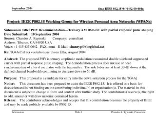
Project: IEEE P802.15 Working Group for Wireless Personal Area Networks (WPANs) Submission Title:PHY Recommendation—Ternary AM DSB-SC with partial response pulse shaping Date Submitted: 10 September 2004 Source: Chandos A. Rypinski Company: consultant Address: Tiburon, CA 94920 USA Voice: +1 415 435 0642 FAX: none E-Mail: chanryp@sbcglobal.net Re: TG4A Call for contributions, Jason Ellis, August 2004 Abstract: The proposed PHY is ternary amplitude modulation transmitted double sideband suppressed carrier with partial response pulse shaping. The demodulation process does not use or need synchronization of a local oscillator with the transmitter. The side lobes are at least 30 dB down at the defined channel bandwidth continuing to decrease down to 50 dB. Purpose: This proposal is a candidate for entry into the down-selection process for the TG4A] Notice: This document has been prepared to assist the IEEE P802.15. It is offered as a basis for discussion and is not binding on the contributing individual(s) or organization(s). The material in this document is subject to change in form and content after further study. The contributor(s) reserve(s) the right to add, amend or withdraw material contained herein. Release: The contributor acknowledges and accepts that this contribution becomes the property of IEEE and may be made publicly available by P802.15. Chandos A. Rypinski, Consultant
PHY Recommendation—Ternary AM DSB-SC (with partial response pulse shaping) Chandos A. Rypinski, consultantwith Bob Ritter and John ArmaniniMicroTech Specialist Chandos A. Rypinski, Consultant
Summary of Desired Properties • An uncommon digital modulation technique is recommended for short-reach, scalable data rate personal area as an alternative to widely used GMSK, BPSK, DPSK and OQPSK modulations. The targeted applications are those requiring a combination of properties which include: • high like-signal interference resistance to enable extensive frequency reuse over a large area, • low sidelobe levels to enable better use of adjacent channels and • the flexibility to trade off channel coding schemes and occupied bandwidth for the best fit to the specific application Chandos A. Rypinski, Consultant
Summary of Proposal • The recommended baseband modulation is amplitude modulated ternary (three amplitude levels) DSB-SC (double-sideband suppressed carrier) with partial response type pulse shaping. • The specific unit-pulse shape (now referred to as “Sym-pulse”) used provides minimized use of low frequencies with zero dc component and low levels of side lobes. Chandos A. Rypinski, Consultant
Advantage Summary A • Zero dc and reduced low frequency energy density below 10% of the high edge frequency of the power density spectrum enables baseband amplification with video rather than dc amplifiers. • Independence of rf phase/frequency at demodulation: 1) great tolerance to motion of the user station2) decreased susceptibility to phase reversal errors with frequency dependent time domain fades. • Low adjacent channel and second channel emissions are the result of using the right pulse shape in the first place, rather than filtering a high side lobe signal. Chandos A. Rypinski, Consultant
Advantage Summary B • Copper pairs can transport the baseband waveform large distances without equalization. • Overhead time used for acquisition is greatly reduced by the absence of the need for rf synchronization. • Twice the average power allowed for BPSK may be used with the specified channel coding. Half the bits are 0's transmitted at zero amplitude creating a 50% duty cycle. Chandos A. Rypinski, Consultant
Property Summary for Ternary DSB-SC • Feasible data rates: 10 Kbps to 32 Mbps • Spectrum zero’s: Zero’s at 0, 0.8 x bit-rate, 1.0 x bit-rate • Occupied bandwidth: @ -10 dB 0.16 to 1.28 x bit-rate @ -20 dB 0.08 to 1.4 x bit-rate @ -30 dB 0.04 to 1.5 x bit rate • Acquisition time: zero time for rf synchronization 120 bits for AGC setting, bit clock acquisition and start delimiting Chandos A. Rypinski, Consultant
The unit pulse defines the spectral characteristics. A number of concatenated, overlapping pulse make up the bit stream. The composite stream has about the same spectrum as the unit pulse. The length of the space between zero crossings at the center is equal to one bit. The unit pulse may be upright or inverted or zero. The Unit Pulse Chandos A. Rypinski, Consultant
The Serial Data Stream at Video Baseband Upper: 130 bits of psuedo random source data Lower: Corresponding Sym-pulse video waveform Chandos A. Rypinski, Consultant
“Eye diagram” The “Eye” diagram shows all transition trajectories between consecutive states. There are two eyes and two decision thresholds (one after squaring) for the Sym-pulse modulation. Chandos A. Rypinski, Consultant
Power Density Spectrum for Data Burst This PSD is for the previously shown video data stream operating at 25 Mbps. This is a mathematical simulation The X-axis is in steps of 5 MHz. The Y-axiz is in steps of 20 dB The first non-zero null is at 20.5 MHz and the second at 25-26 MHz Chandos A. Rypinski, Consultant
Power Density Spectrum from Analyzer Screen Capture This figure is the DSB radio signal at 5.25 GHz. The X-axisgrid is in steps of 10 MHz. The Y-axis is is steps of 10 dB. Chandos A. Rypinski, Consultant
Power Density Spectrum from System Simulation DSB-SC at 25 Mbps X-axis: 20 MHz/div Y-axis: 10 dB/div CF: 5.250 GHz Chandos A. Rypinski, Consultant
Radio Implementation Block Diagram This radio operates at 5.25 GHz with a first IF of 400 MHz. It is double sideband suppressed carrier. The modulator-demodulator-detector function is shown in the central blue box. The data rate is up to 32 Mbps in 50 MHz. Chandos A. Rypinski, Consultant
The Value of Phase/frequencyIndependent AM Modulation A typical room coverage appears to contain coverage holes due to cancellation of the predominant path rays. When a cancellation fade is traversed in time frequency or space, the rf phase is usually reversed between entering and leaving. While increased transmitter power will moderately decrease the hole size, it rarely will make the hole disappear. An rf phase reversal can shake loose a PLL which will then take many bit times to recover causing a “hit” type data error. A similar difficult can exist in a mathematical de-rotator. When a cancellation null is encountered, there may be a substantial recovery time if PLL loops are use to recover virtual carrier (e.g., Costas loop). This difficult can be overcome by using differential QPSK where the phase reference for the current pulse is the preceding pulse. Since the reference has the same noise as the signal there is a small loss S/N threshold, but many have thought it worthwhile for the reduction in size of hit errors. Chandos A. Rypinski, Consultant
Frequency Independent Amplitude Demodulation (1) The amplitude detector is based on using an vector (I-Q) demodulator which may be at an intermediate or signal frequency. The output processing is based on the identity: sin²(θ)+cos²(θ) = 1 The I and Q outputs are separately squared and the two results summed to obtain a phase-independent measure of the signal amplitude. The squaring operation yields a single positive output for either phase in the source signal, and it provides an amplitude indication proportional to signal power and independent of phase angle. Chandos A. Rypinski, Consultant
Frequency Independent Amplitude Demodulation (2) The data demodulator assumes use of an approximate AGC which is set at the start of the burst preamble and refreshed during the message. A second forward acting level compensator sets the threshold in relation to the peak signal level. The threshold is set at about 70% of the reference level for a comparator device which at sampling time determines the level to be above or below threshold. There is an integrate-and-dump circuit which sums the areas of the central half of the incoming bit-pulse. The integration capacitor is sampled at the end of the charge interval and it is discharged during the non-integrate interval. The block diagram of this type of demodulator appears in the radio block diagram of Figure 8. This block diagram has been simulated end-to-antenna-path-antenna-to-end in same simulator as used for Figure 5. Chandos A. Rypinski, Consultant
Closing Summary (1) We propose that the TG4A committee accept Ternary AM DSB-SC with partial response pulse shaping as a candidate for the opening PHY layer selection. Anyone can propose, but only a majority constituency can select. Any opening recommendation is likely to be substantially modified before it is acceptable for incorporation in the standards document. If selected, we will do everything necessary to enable a multi-vendor environment according to IEEE Standards Rules. We plan to build a small number of technology demonstrator’s which are now being designed. These could be available for independent verification of properties in December 2004 or soon after. Chandos A. Rypinski, Consultant
Closing Summary (2) • This proposal offers a competent function, implemented with smallest and simplest circuit function. It is one of the best for: • transmitter power utilization • resistance to like and foreign signal interference • minimal out-of-band side lobe levels • resistance to errors from multipath including moving reflectors (one of only a few modulations with this property) • accurate transmission without forward error correction • fast and simple clock acquisition • Please join us in supporting the choice of this modulation Chandos A. Rypinski, Consultant