Timers
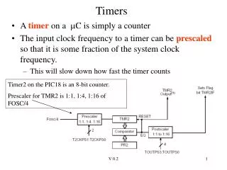
Timers. A timer on a C is simply a counter The input clock frequency to a timer can be prescaled so that it is some fraction of the system clock frequency. This will slow down how fast the timer counts. Timer2 on the PIC18 is an 8-bit counter.

Timers
E N D
Presentation Transcript
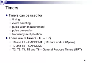
Timers • A timer on a C is simply a counter • The input clock frequency to a timer can be prescaled so that it is some fraction of the system clock frequency. • This will slow down how fast the timer counts Timer2 on the PIC18 is an 8-bit counter. Prescaler for TMR2 is 1:1, 1:4, 1:16 of FOSC/4 V 0.2
Period Register • A timer can be programmed to roll over at any point using the period register. • An 8-bit timer would typically roll over to 0x00 once it reached 0xFF. • However, if the period register is set to 0x7F, then timer will roll over to 0x00 once it increments past 0x7F. PR2 is the period register for TMR2 V 0.2
Postscaler • Would like to generate an interrupt when a timer rolls over • A Postscaler is used as a second counter – only generate an interrupt after timer rolls over N times. Postscaler – all values from 1:1 to 1:16. V 0.2
PIC18 Timer Summary • Timer0: software selectable as either 8-bit or 16-bit, has a prescaler, clocked by FOSC/4 or external clock. • Timer1: 16-bit, has a prescaler, used with capture/compare module, clocked by FOSC/4 or external clock (has dedicated oscillator circuit, so can support a second external crystal). • Timer2: 8-bit, has prescaler/period register /postscaler, used with pulse-width modulation module • Timer3: A duplicate of Timer 1, shares Timer1’s dedicated oscillator circuit. • Capture/Compare module • 16-bit capture register, 16-bit compare register • Used with timer1 or timer3 to provide additional time measurement capabilities V 0.2
So....what good are timers? • Better than Ginzu knives – a 1001 uses! • Usage #1 – generate an interrupt at fixed frequency • Square wave generation • Sampling an input signal with A/D I bought a set of Ginzu knives for only three easy payments of $29.95 and they came with a lifetime guarantee. When the handles fell off, I returned the knives with my lifetime guarantee asking for a refund. They wrote back saying, "The guarantee was for the lifetime of the knives. Obviously, the knives are dead, so the guarantee is no longer valid." (internet humor) V 0.2
Square Wave Generation One method: Generate a periodic interrupt at ½ the period time. Complement an output port each interrupt time. This will generate a square wave with a 50% duty cycle. interrupt interrupt interrupt Low Pulse width (LPW) RBx High Pulse width (HPW) Period duty cycle = HPW/Period * 100% Frequency = 1/Period V 0.2
Example Assume a 10MHz oscillator frequency. Generate a square wave with a 1KHz frequency. Period = 1.0 /1KHz = 1/1000 = 0.001 = 1 ms (1 millisecond) Interrupt every 0.5 ms or 500 s (interrupt frequency = 2 KHz) Timer2 interrupt interval = Pre * (PR2+1) * Post * (1/(Fosc/4)) IF (interrupt freq = 1/[Pre * (PR2+1) * Post * (1/(Fosc/4))] PR2 = ( 1/[Pre * IF * Post * (1/(Fosc/4))]) - 1 where Pre is prescaler (1, 4, 16), PR2 is period match register, Post is postscaler This is an equation with THREE unknowns! Multiple solutions. Use a spreadsheet! V 0.2
Spreadsheet No solution for Postscale=1, Prescale =4, PR2 too large. No solution for Postscale=Prescale =1, PR2 too large. V 0.2
Pulse Width Modulation Pulse Width Modulation (PWM) is a common technique for controlling average current to a device such as a motor. PIC RBx RBx High Pulse width (HPW) For a fixed frequency, the brightness of the LED will vary directly with duty cycle. The higher the duty cycle (the longer the high pulse width), the brighter the LED because it stays on longer (more current delivered to the LED) V 0.2
PWM Motor Control Base +30V Collector PIC Emitter RBx DC motor NPN BJT Power Transistor Duty cycle applied to Base terminal controls current. The base-to-emitter circuit looks like a diode to the PIC. Gain of the NPN and base current determines maximum current delivered. V 0.2
Capture/Compare/PWM Module • Each CCP Module contains • 16-bit Capture Register, 16-bit Compare Register • PWM Master/Slave Duty Cycle Register • PWM mode is used to produce a square wave without processor intervention • Uses timer2 resource, and Compare register • Square wave on output pin 100% hardware generated, no software intervention • Can vary the duty cycle via the Timer2 PR2 register V 0.2
PIC18Fxx2 PWM CCPR1H, CCPR1L are the upper/lower bytes of compare register Square wave appears here. V 0.2
PIC18Fxx2 PWM Period Period = (PR2+1) * 4 * (1/Fosc) * TMR2_Prescale Note that when TMR2 is used for PWM, the postscaler is NOT used. V 0.2
PIC18Fxx2 PWM Duty Cycle Duty cycle has 10-bit resolution, upper 8-bits in CCPR1L, lower two bits are CCP1CON<5:4> CCPR1H used to double buffer the PWM operation. When TMR2=PR2, output SET, TMR2 reset to 0. When TMR2 = CCPR1H, then output RESET V 0.2
PIC18Fxx2 PWM Duty Cycle Duty Cycle = CCPR1L:CCPCON<5:4> * (1/Fosc) * TMR2_prescale 10 bits. Recap: Period defined by PR2, duty cycle by CCPR1L + 2 bits The duty cycle time should be less than the period, but this is NOT enforced in hardware. If duty cycle > Period, then the output will always be a high (will never be cleared) V 0.2
sqwave.c Generate a square wave using TMR2 and the PWM. bitclr(T2CON, 6); /* TMR2 post scale =1 */| bitclr(T2CON, 5);bitclr(T2CON, 4);bitclr(T2CON, 3); bitclr(T2CON, 1); /* TMR2 pre scale of 4 */bitset(T2CON, 0); bitset(T2CON, 2); /* start timer 2 */ /* set up PWM */ PR2 = 255; /* set timer2 PR register */CCPR1L = (255 >> 1); /* 50% duty cycle */ bitclr(CCP1CON, 5); /* lower 2 bit= 00 */bitclr(CCP1CON, 4); V 0.2
sqwave.c (cont) /* set CCP1 output */ bitclr(TRISC,2); /* output mode */ /* PWM Mode */ bitset(CCP1CON, 3); bitset(CCP1CON, 2); bitclr(CCP1CON, 1); bitclr(CCP1CON, 0); while (1) { /* prompt user, allow user to change period by changing PR2) */ } At this point, the square wave is active, no other intervention necessary. V 0.2
ledpwm.c Use potentiometer and PIC A/D to adjust duty cycle for PWM to LED Analog input PIC Vdd AN0 CCP1 10K Pot. Use this adjust duty cycle Will initialize PWM module in the same way as before, except TMR2 interrupt will be enabled. In ISR, read A/D value and update duty cycle. V 0.2
ledpwm.c (cont) void interrupt timer2_isr(void) { update_pwm(); TMR2IF = 0; //clear timer2 interrupt flag } This subroutine does work of reading A/D and changing the duty cycle. V 0.2
ledpwm.c (cont) update_pwm(){ unsigned char rval1; rval1 = ADRESH; /* A/D value left justified*/ CCPR1L = rval1; /* upper 8 bits of duty cycle */ rval1 = ADRESL; /* update lower two bits of duty cycle */ if (bittst(rval1,7)) bitset(CCP1CON, 5); else bitclr(CCP1CON, 5); if (bittst(rval1,6)) bitset(CCP1CON, 4);| else bitclr(CCP1CON, 4); /* start new conversion */ bitset(ADCON0, 2); /* start conversion */ } V 0.2
sinegen.c Analog input Vdd Sinewave Maxim 517 PIC Vdd OUT1 OUT0 RA0/AN0 AD1 SCL RC3/SCK/SCL AD0 10K Pot. RC4/SDI/SDA SDA Potentiometer used to vary the PR2 timer value between a min value of 25 and max value of 100. This varies TMR2 interrupt time. Sinewave is produce by table look-up (either 16-entry table or 64-entry table). Period of Sinewave is number_table_entries * tmr2_interrupt_interval. V 0.2
16 Entry Table const unsigned char sine16tab[] = {0x80,0xb0,0xda,0xf6,0xff,0xf6,0xda,0xb0,0x80,0x4f,0x25,0x9,0x0,0x9,0x25,0x4f}; V 0.2
Period TMR2 interrupt interval. New entry read from table each interrupt. Period = 16 * TMR2 interrupt interval. V 0.2
Saving Data Space • 64-entry table is same as 16-entry, just finer grain • Both end up being stored in File Register memory (Bank1) • Could save File Register memory by noting that really only have to save ¼ of the waveform 2nd quarter is 1st quarter read in reverse order. 3rd quarter = 1st – 0x80 4th quarter = 1st – 0x80 read in reverse order 1st 2nd 3rd 4th 0x80 V 0.2
sinewave.c (main loop) for(;;) { if(dac_flag) { if (tabmax == 16) update_dac(sine16tab[sineptr]); else update_dac(sine64tab[sineptr]); dac_flag = 0; if (pr_flag) { update_period(); pr_flag = 0; } }} dac_flag set by ISR tabmax chooses between 16-entry, 64-entry tables. Read value out of table, update DAC. pr_flag set by ISR when at end of period (16 or 64) Read A/D to get new TMR2 interval, update PR2 V 0.2
sinewave.c (ISR) void interrupt timer2_isr(void) { sineptr++; if (sineptr == tabmax){ sineptr = 0; pr_flag = 1; } dac_flag = 1; TMR2IF = 0; clear timer interrupt flag } Move to next entry in table Reset if at end of table Signal to main loop that end of period reached, need to update period Signal to main loop that interrupt occurred. Clear TMR2 interrupt flag so interrupt can happen again. V 0.2
Read A/D, get upper 8 bits, clip to between MIN/MAX. – this code would be simpler if right justification used. sinewave.c (update_period) update_period(){ unsigned char rval1,rval2; /* read ADC result, use as period, start new conversion */ rval2 = ADRESL >> 3; /* lose lower 3 bits */ rval2 = rval2 & 0x1f; /* mask upper 3 bits */ rval1 = ADRESH & 0x3; /* mask upper 6 bits */ rval1 = rval1 << 5; rval1 = rval1 | rval2; if (rval1 < MIN_PERIOD) rval1 = MIN_PERIOD; if (rval1 > MAX_PERIOD) rval1 = MAX_PERIOD; PR2 = rval1; /* set timer2 period register */ /* start new conversion */ bitset(ADCON0, 2); /* start conversion */ } Set new PR2 value, start new conversion. V 0.2
Experiment 11 Task: Waveform Generation Generate a waveform that consists of 1 or more sine wave cycles, 1 or more triangle wave cycles, 1 or more square wave cycles. A 1x period is defined as 64 * TMR2 interrupt interval – sine wave will ALWAYS have a 1x period (use 64 table lookup). Square wave and Triangle waves can have a period of 0.5X (32 intervals), 1.0X (64 intervals) or 2.0X (128 intervals). Square wave/Triangle wave can also be inverted. V 0.2
1x 1x 1x Waveform Examples 64 tmr2 interv. 64 tmr2 interv. 64 tmr2 interv. 1x, inverted 1x, inverted 1x 64 tmr2 interv. 64 tmr2 interv. 64 tmr2 interv. V 0.2
Waveform Examples 0.5x 2x 1x 64 tmr2 interv. 128 tmr2 interv. 32 tmr2 interv. Your assigned waveform is fixed in terms of type of component waveforms, and inversion. To generate square wave/triangle wave – could use table lookup, but probably not enough File register space. Both square wave and triangle wave values are easy to ‘compute’ based on current value and sample number. V 0.2
Triangle Wave Computation Non-inverted 1st 2nd 3rd In 1st, 3rd sections: new_value = old_value + delta In 2nd section: new_value = old_value - delta Delta depends on number of points (period) of waveform. Be careful of wrap-around at low/high points (0x00, 0xFF). V 0.2