Download
1 / 29
300 likes | 716 Vues
Edson P. Bellido Sosa. Corrugation of graphene. Outline. Introduction Purpose and impact Structure of graphene Suspended Over Ru Over SiO 2 Electrical transport Future research Conclusion. Introduction.

E N D
Edson P. Bellido Sosa Corrugation of graphene
Outline • Introduction • Purpose and impact • Structure of graphene • Suspended • Over Ru • Over SiO2 • Electrical transport • Future research • Conclusion
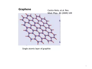
Introduction • Graphene is a one-atom-thick planar sheet of sp2 bonded carbon atoms that are packed in a honeycomb lattice. • Semi-metal with very high electron mobility at 300K (15000 cm2/Vs). • Very high thermal conductivity (5000W/mK). • Very high Young’s modulus (0.5TPa). • In graphene the electrons behave as massless relativistic particles (Dirac fermions) http://www.lbl.gov/Science-articles/Archive/sabl/2007/Nov/assets/img/lrg/graphene_sheet.jpg • Due to its extraordinary properties graphene has many potential applications such: • Single molecule detection. • Graphene transistors • Transparent conductive electrodes • Ultracapacitors • Could be the replacement of Silicon for future electronics
Introduction • According to the Mermin-Wagner theorem crystalline membranes like graphene can exist but they should be rippled. • According to the Mermin-Wagner theorem crystalline membranes like graphene can exist but they should be rippled. • These ripples were observed in graphene and it is believed that they play an important role in its electronic properties. • Intrinsic rippling has been proposed as one of the possible mechanisms for electron scattering to explain the variation in the resistivity with the number of charge carriers experimentally seen in graphene. • The corrugation and electronic properties of graphene can also be influenced by the substrate where the experiments is carried out. • The fabrication method can also influence the corrugation of graphene especially if the method introduce oxygen addends. http://www.thp.uni-koeln.de/graphene08/wavy-graphene.jpeg
Outline • Introduction • Purpose and impact • Structure of graphene • Suspended • Over Ru • Over SiO2 • Electrical transport • Future research • Conclusion
Purpose and Impact PURPOSE • We study the formation of corrugations on graphene sheets and analyze the stability of 2D crystals. • We analyze how the substrate were the graphene sheet is supported will affect the formation of corrugations. • We study how the corrugation affects the electrical transport of the graphene sheets. IMPACT • To exploit graphene as a possible substitute for silicon in electronics we need to understand the structure of graphene and how this structure could be affected by the substrate were is supported. • The understanding of this effect will lead us to the control of the electrical, mechanical and optical properties of graphene changing only the substrate or the environment where the device is going to operate without the necessity of chemical modification that is very difficult to do in a chemically stable carbon structure as graphene.
Outline • Introduction • Purpose and impact • Structure of graphene • Suspended • Over Ru • Over SiO2 • Electrical transport • Future research • Conclusion
Structure of suspended graphene • The central part of the suspended graphene normally appear on TEM images as homogeneous and featureless regions (arrows). • The edges tend to scroll. Also folded regions are observed. • The folds provide a clear TEM signature for the number of graphene layers. • Folded graphene is locally parallel to the electron beam. • Monolayer graphene fold exhibits only one dark line (a). • Bilayergraphene fold exhibits two dark lines (b). 2nm 2nm 500nm Meyer, JC Geim, AK Katsnelson, MI Novoselov, KS Booth, TJ Roth. “The structure of suspended graphene sheets” NATURE March 2007, 446,7131, 60-63
Structure of suspended graphene • Monolayer graphene can be directly distinguish by analyzing nanobeam electron diffraction patterns from their flat areas as a function of incidence angle. This allow us to procedure effectively the whole 3D reciprocal space (c-e). • For graphene monolayer changes in the total intensity are relatively small and, importantly, there are no minima (f). • For bi-layer graphene the total intensities vary so strongly that the same peaks become completely suppressed at some angles and the underlying sixfold symmetry remains undisturbed only for normal incidence (g). • The diffraction peaks for the monolayer become broader with increasing tilt angle and this blurring is much stronger for those peaks that are further away from the tilt axis. In disagreement with the calculated intensities (dashed lines) Meyer, JC Geim, AK Katsnelson, MI Novoselov, KS Booth, TJ Roth. “The structure of suspended graphene sheets” NATURE March 2007, 446-7131, 60-63
Structure of suspended graphene • The observed broadening explicitly reveals that graphene sheets are not flat. • The full 3D Fourier transform of a flat graphene crystal (a) consists of a set of rods perpendicular to the plane of the reciprocal hexagonal lattice (c). • In particular, this picture suggests that the intensity of diffraction peaks monotonically change with tilt angle. • The increasing broadening of diffraction peaks without changes in their total intensity implies that the rods wander around their average direction (d). This corresponds to a slightly uneven sheet (b). • Such roughness results in sharp diffraction peaks for normal incidence, but that the peaks rapidly become wider with increasing tilt angle (e). Meyer, JC Geim, AK Katsnelson, MI Novoselov, KS Booth, TJ Roth. “The structure of suspended graphene sheets” NATURE March 2007, 446-7131, 60-63
Structure of suspended graphene • Figures f and g show the detailed evolution of the broadening of the diffraction peaks with changing incidence angle. • The peak widths increase linearly with tilt and also proportionally to the peaks' position in reciprocal space, in quantitative agreement with the simulations for corrugated graphene. • The width of the cones in f and g provide a direct measure of the membrane's roughness. For different monolayers the cone angles were between 8° and 11°. For bilayer membranes, this value was found to be about 2° (g). • The corrugations are less than or equal to 25 nm with a height about 1 nm. Importantly, atomic-resolution images show that the corrugations are static, because otherwise, changes during the exposure would lead to blurring and disappearance of the additional contrast. Meyer, JC Geim, AK Katsnelson, MI Novoselov, KS Booth, TJ Roth. “The structure of suspended graphene sheets” NATURE March 2007, 446-7131, 60-63
Outline • Introduction • Purpose and impact • Structure of graphene • Suspended • Over Ru • Over SiO2 • Electrical transport • Future research • Conclusion
Structure of graphene over Ru • Monolayer graphene is epitaxialy growth on Ru (0001). • Figure a shows that monoatomic steps and dislocations of the substrate are reproduced by the graphene layer. • Figure b shows a STM topographic image of graphene showing the formation of ripples. The inset is a Fourier transformation of the image. • The ripples height are approximately 0.02nm (d). • Figure c shows the structure model. Vazquez de Parga, A. L. and Calleja, F. and Borca, B. and Passeggi, M. C. G. and Hinarejos, J. J. and Guinea, F. and Miranda, R. “Periodically Rippled Graphene: Growth and Spatially Resolved Electronic Structure “. Phys. Rev. Lett. 100, 056807,2008
Structure of graphene over Ru • Figure a shows spatially resolved dI/dV tunneling spectra, which are roughly proportional to the local density of states (LDOS), recorded on top of the ‘‘high’’ and ‘‘low’’ regions of the corrugated graphene layer. Figure b shows the corresponding calculation. • The left and right images in the upper panel are maps of dI/dV at 100 meV and 200 meV and reflects the spatial distribution of the LDOS below and above the Fermi level, respectively. • The central image shows the topographic image recorded simultaneously. The lower panel shows the corresponding calculations for the spatially resolved LDOS for a periodically corrugated graphene layer. Vazquez de Parga, A. L. and Calleja, F. and Borca, B. and Passeggi, M. C. G. and Hinarejos, J. J. and Guinea, F. and Miranda, R. “Periodically Rippled Graphene: Growth and Spatially Resolved Electronic Structure “. Phys. Rev. Lett. 100, 056807,2008
Structure of graphene over Ru • Figure a is a 10 nm x 10 nm atomically resolved STM image of a graphene island on Ru(0001). The inset shows an image of the whole island with a lateral size of 47 nm. • Figure b shows spatially resolved tunneling spectra measured on the high (black curve) and low (red curve) areas of the ripples close to the edge of the island and on clean Ruthenium (blue curve). • The spectrum recorded on clean Ru patches show indeed only the surface state around the Fermi energy observed on Ru(0001). Vazquez de Parga, A. L. and Calleja, F. and Borca, B. and Passeggi, M. C. G. and Hinarejos, J. J. and Guinea, F. and Miranda, R. “Periodically Rippled Graphene: Growth and Spatially Resolved Electronic Structure “. Phys. Rev. Lett. 100, 056807,2008
Outline • Introduction • Purpose and impact • Structure of graphene • Suspended • Over Ru • Over SiO2 • Electrical transport • Future research • Conclusion
Structure of graphene over SiO2 • Figure a shows the topography of graphene deposited on SiO2. The square indicates the region shown in c. The wide white line is an electrical contact. • Figure c shows the graphene sheet. The standard deviation of the height variation in a square of side 600 nm is approximately 3 Å. 300nm 500nm MasaIshigami, J. H. Chen, W. G. Cullen, M. S. Fuhrer, and E. D. Williams. “Atomic Structure of Graphene on SiO2 “. NanoLett. Vol7, 1643-1648,2007
Structure of graphene over SiO2 • An atomic-scale image is shown in figure a, with a height variation of 2.5nm, and can be imaged clearly at higher resolution as shown in parts b and d. • The meandering of atomic rows seen in figure d is due to the curvature of the surface. • The appearance of both triangular and hexagonal lattice in the image indicates the presence of strong spatially dependent. • perturbations which interact with graphene electronic states. Such perturbations may be due to film curvature and/or the charge traps on the SiO2 surface. 2.5Å 2nm 2.5Å 2.5Å MasaIshigami, J. H. Chen, W. G. Cullen, M. S. Fuhrer, and E. D. Williams. “Atomic Structure of Graphene on SiO2 “. NanoLett. Vol7, 1643-1648,2007
Structure of graphene over SiO2 • Figure a shows an AFM image of the boundary between the graphene sheet and SiO2 substrate. • An histogram acquired across the boundary shown in figure b shows that the film thickness is 4.2 Å, comparable to the layer-to-layer spacing in bulk graphite of 3.4 Å. Therefore, the imaged graphene device area is a monolayer. • Figure c shows histograms of the heights over graphene and SiO2. The graphene sheet is approximately 60% smoother than the oxide surface. MasaIshigami, J. H. Chen, W. G. Cullen, M. S. Fuhrer, and E. D. Williams. “Atomic Structure of Graphene on SiO2 “. NanoLett. Vol7, 1643-1648,2007
Structure of graphene over SiO2 • The height-height correlation function g(x)=(z(x0 + x) - z(x0))2, is shown in figure d. • Both correlation functions rapidly increase as g~x2H at short distances 2H=1.11 for graphene and 2H=1.17 for SiO2. A value of the exponent 2H~1 indicates a domain structure with short range correlations among neighboring domains. • The observed 2H value demonstrates that the observed graphene morphology is not representative of the intrinsic structure. • Interpolating the intersection of the power law and saturated regimes yields values of the correlation length, which are ξ=32nm for graphene and ξ=23nm for SiO2. • The larger correlation length and smaller roughness of the graphene surface would arise naturally due to an energy cost for graphene to closely follow sharp orientation changes on the substrate. MasaIshigami, J. H. Chen, W. G. Cullen, M. S. Fuhrer, and E. D. Williams. “Atomic Structure of Graphene on SiO2 “. NanoLett. Vol7, 1643-1648,2007
Outline • Introduction • Purpose and impact • Structure of graphene • Suspended • Over Ru • Over SiO2 • Electrical transport • Future research • Conclusion
Electrical transport of graphene • A 42 atom graphene ribbon with zigzag edges is contacted through a single sulfur atom to finite gold electrodes. The electrodes are oriented along the (111) direction and are described by clusters with finite cross sections. The vertical distance between the sulfur atom and the most external plane of the gold electrodes is 1.90 Å with an S–Au bond length of 2.53 Å. The other bond lengths used here are Au–Au (2.88 Å), S–C (1.97 Å), and C–C (1.42 Å). • The geometry of the nonperfectly flat ribbons is obtained by molecular dynamics simulations using Tersoff’s potential.
Electrical transport of graphene • From the DOS of the two structures one can observe few differences. First, for corrugated graphene, there is an increase in the number of peaks in the DOS above EF and a decrease below it as compared to the DOS of the flat surface. • Second, the heights of peaks are different for the two structurally different graphene flakes. In general, the amplitude of the DOS peaks at around EF for the flat structure is larger than that of the corrugated case. • For flat graphene the Fermi level lies in a gap, it crosses a region of finite DOS in the corrugated case. • The DOS peaks at around EF, for the corrugated structure is broader than the flat one.
Electrical transport of graphene • The electron transmission is investigated for a wide energy region around the Fermi level. • There is a considerably larger transmission coefficient at the Fermi level for the corrugated flake with respect to the flat one. This directly follows from the fact that a finite DOS at EF is present only for corrugated ribbons, while for the flat ones, this is absent, and the transmission can only be tunneling like. • There is a much higher peak in transmission just below EF for the corrugated ribbon with respect to the flat one. However, the reversal is observed between −7.5 and −9 eV.
Electrical transport of graphene • The I-V characteristics show that the corrugated flakes display a large low-bias current, which linearly increases with a bias of up to 0.2 V for both current polarities. Nonlinearity sets in at a higher bias of ±0.2 eV. Then, it saturates at a value around 25µA. • The I-V of the flat graphene flake is considerably lower at any bias investigated and increases with bias in a rather nonlinear way. These phenomena mean that the barrier for electron transport for the devices with corrugated graphene is reduced and the current-carrying capabilities are increased compared to the flat one.
Outline • Introduction • Purpose and impact • Structure of graphene • Suspended • Over Ru • Over SiO2 • Electrical transport • Future research • Conclusion
Future Research • Analysis of electrical properties of graphene on different substrates. • Analysis of the relation between corrugation and optical and mechanical properties of graphene. • Study of more substrates and how these substrates affects the formation of corrugations • Fabrication of patterns with different materials to use as substrate of graphene and take advantage of the difference in the formation of corrugation and the difference in electrical properties due to structural change in graphene. • Study of the formation of corrugations on solutions. • Study of the interactions of graphene sheets with molecules and how this affect the structure of graphene. • Analysis of changes in the band gap when changing the formation of corrugations.
Outline • Introduction • Purpose and impact • Structure of graphene • Suspended • Over Ru • Over SiO2 • Electrical transport • Future research • Conclusion
Conclusions • The study of suspended graphene confirm that the corrugations are intrisic to graphene sheets. This confirm the termodynamic stability of defect free 2D structures with out-of-plane deformations involving a significant elastic strain. • It is possible to produce highly perfect, spatially extended, graphenemonolayers and islands on Ru(0001). The graphene sheets present corrugations that produce a spatial charge redistribution. The graphene sheets present ripples due to surface roughness however it still presents well defined intrinsic corrugations. • The observation of graphene sheets over SiO2 shows that the graphene primarily follows the underlying morphology of SiO2 and thus does not have intrinsic, independent corrugations on SiO2. • The transmission through the corrugated graphene flake is considerably higher than that across a perfectly flat surface. As a consequence, the I-V characteristics are rather different in the two cases, with a linear behavior followed by current saturation for the corrugated flake. • Graphene sheets present intrinsic corrugations however the degree of deformation is determined principally for the substrate where the sheet is supported.