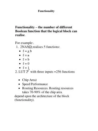
Functionality
Functionality. 3. 2. The functionality of the block and the effectiveness of the use of the chip area. Example. Let us realise the function f = abc + bcd + a b c. Two-input LUT-s – 32 memory bits and 17 connections. a. AND. b. AND. c. b. AND. OR. c. AND. d. a. OR. AND. b.

Functionality
E N D
Presentation Transcript
Functionality 3 2
The functionality of the block and the effectiveness of the use of the chip area
Example. Let us realise the function f = abc + bcd + a b c Two-input LUT-s – 32 memory bits and 17 connections a AND b AND c b AND OR c AND d a OR AND b AND c Three-input LUT-s - 32 s memory bits and 13 connections a b AND c b c OR AND d a b AND c Four input LUT-s - 16 memory bits and 5 connections a b c d
Logical blocks based on LUT-s LUT 0 T MUX 1 S LUT 0 T MUX 1 S k Area of the logical block LBA = FA + (M BA 2 ) x x LBA –area of the logical block FA – fixee area M – number of LUT-s BA – area of the bit
Geometrical model W RP CL X Logical block CL CL + ( ) W RP X W RP X RP – Routing Piich Symmetrical FPGA. 2 RALB = 2(CL W RP) + (W RP) x x x RALB – Routing Area per LB Row Based FPGA. RALB = CL W RP x x Total area Total Area = Nblock (LBArea + RALB)
Logical blocks with decomposable LUT-s . The number of LUT bits is constantly 5 . M=1 IN1 LUT OUT . . . IN5 M=2 IN1 LUT . . . IN4 0 MUX OUT 1 IN5 s LUT . . . IN9 IN10
Logical blocks with decomposable LUT-s II M=4 IN1 LUT IN2 IN3 00 MUX OUT IN4 LUT 01 IN5 IN6 10 IN7 LUT 11 IN8 s0 s1 IN9 IN10 LUT IN11 IN12 IN13 IN14
Logical blocks with decomposable LUT-s III M=8 IN1 LUT IN2 000 MUX OUT IN3 LUT 001 IN4 010 IN5 LUT 011 IN6 100 IN7 LUT 101 IN8 110 IN9 LUT 111 IN10 s0 s1 s2 LUT IN11 IN12 LUT IN13 IN14 LUT IN15 IN16 IN17 IN18 IN19
Experimental results: • Summary of the functionality and area-effectiveness of the logical block: • One-output LUT is the best while K=4 • Pins waste area. The best solution is large functionality per pin. • LUT with several outputs is not effectual. • The best block based on PLA has 8-10 inputs, 12-13 terms and 3-4 outputs. • In case of decomposable LUT-s the best solution is M=4 • Adding trigger to the logical block is effectual
Functionality of the logical block and its performance • If functionality increases: • 1. the number of levels (logical blocks) decreases at the pathofthe signals; • 2. the delay of the logical blocks increases (bigger and more complex); • 3. the total routing delay decreases; • 4. total delay ? Dtot = Nl (Dlb + Dr) x Dtot –total delay Dlb – delay of the logical block Dlb –delay of routing Nl – number of logical blocks at the critical path
Example. Two different realisations of the function f = a d b + a b c + a c d The logical blocks contain NAND elements with two outputs a & & b & & & c d & a & & c & & d The logical blocks contain three-input LUT-s a b d a b c a c d 2NAND delay 0,7 ns 3-LUT delay 1,4 ns Routing delay >0 LUT is swifter
Summary concerning the functionality and speed of the logical block • LUT with 5-6 inputs is good in case of a medium-sized routing delay • Low functional logical blocks (such as 2NAND) are not swift; • It is effectual to add the inversion possibility in case of simple logical blocks. • It is effectual to increase the number of terms from three to five in case of large • AND-OR blocks
Summary • Logical blocks with a very low level of functionality are not good both from the point of view of speed and functionality; • Large functionality per output is good (e.g LUT-s) • The best LUT is with 4 inputs; • The best logical block from the point of view of area is the one where PLA structures are used; • Decomposable LUT-s can be effectual in solving some type of tasks; • Non-homogenuous structures can be more useful than homogenuous; • Hierarchical FPGA organisation may be more effective than a single-level organisation